
19 Jan Chips to Start-up (C2S) Programme: India’s Design-Led Semiconductor Transformation
This article covers “Daily Current Affairs” and From Chips to Start-up (C2S) Programme: India’s Design-Led Semiconductor Transformation
SYLLABUS MAPPING
GS- 3- Science and Technology- Chips to Start-up (C2S) Programme: India’s Design-Led Semiconductor Transformation
FOR PRELIMS
What is the Chips to Start-up (C2S) Programme?
FOR MAINS
What do you understand by the Chips to Start-up (C2S) Programme?
Why in the News?
India’s semiconductor chip design ecosystem is in the news due to the rapid scaling up of government-led skill and design initiatives under MeitY, particularly the Chips to Start-up (C2S) Programme and the Design Linked Incentive (DLI) Scheme. With nearly 400 organisations—including 305 academic institutions and 95 startups—now engaged, these initiatives aim to bridge the global semiconductor talent gap, strengthen design-led innovation, and position India as a key player in the global semiconductor value chain amid rising demand for AI, advanced electronics, and high-performance computing.

Overview: Chips to Start-up (C2S) Programme
The Chips to Start-up (C2S) Programme is a flagship capacity-building initiative launched by MeitY in 2022, with a total outlay of ₹250 crore over five years, covering academic institutions across the country.
The programme aims to develop 85,000 industry-ready professionals across undergraduate, postgraduate, and doctoral levels, including:
1. 200 PhD scholars engaged in advanced chip design research
2. 7,000 M.Tech graduates specialising in VLSI or Embedded Systems
3. 8,800 M.Tech graduates from computer, communication, and electronic systems disciplines with focused VLSI exposure
4. 69,000 B.Tech students trained through VLSI-oriented coursework
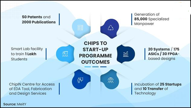
Beyond human resource development, the C2S Programme seeks to catalyse innovation and entrepreneurship by:
1. Incubating 25 semiconductor start-ups
2. Enabling 10 technology transfers
3. Providing access to SMART laboratory facilities
4. Training over one lakh students
5. Generating 50 patents
6. Supporting 2,000 focused research publications
Programme Approach and Implementation
The C2S Programme adopts a hands-on, end-to-end learning model, providing students with practical exposure to chip design, fabrication, and testing. This is achieved through structured training programmes conducted in collaboration with industry partners, supported by continuous mentorship and access to advanced infrastructure.
Participants gain access to state-of-the-art Electronic Design Automation (EDA) tools, semiconductor foundries, testing facilities, and high-performance computing resources. Students undertake R&D projects to design and develop Application-Specific Integrated Circuits (ASICs), Systems-on-Chip (SoCs), and Intellectual Property (IP) cores, enabling them to bridge theoretical learning with real-world semiconductor design workflows.
Institutional Participation Framework for Semiconductor Chip Design (India)
| Tier / Category | Institutions / Organisations Covered | Key Support Provided | Major Activities | Outcomes / Exposure |
|---|---|---|---|---|
| Core Academic Institutions | 100+ Participating Academic Institutions | Project funding, EDA tools, specialised training | R&D projects in chip design & fabrication (2–5 years); curriculum integration; labs; student projects; short-term courses | End-to-end exposure to chip design, fabrication, testing; development of indigenous chip solutions |
| Other Participating Organisations | 200+ Academic & Training Organisations | Access to EDA tools and training support | Curriculum instruction; short-term courses; hands-on labs; design projects | Exposure to standard chip design flows using advanced EDA tools |
| National Design Infrastructure | ChipIN Centre, C-DAC Bengaluru (serving 300+ institutions) | Advanced design facilities; industry-grade EDA tools | Regular industry-led training programmes; hands-on design workshops | High-quality skill development; industry-aligned chip design capability |
| Capacity Building & Skill Labs | SMART Labs, NIELIT (including Calicut; pan-India access) | Centralised hardware resources; certification platforms | Short-term courses; certification programmes; practical training | Scalable nationwide access to semiconductor design training |
| Technology Enablement – EDA Tools | Global EDA & tech partners | Advanced design & simulation software | Chip architecture design, verification, testing, and optimisation | Industry-standard design competence |
| Technology Enablement – Foundry Access | SCL Mohali, IMEC, MUSE Semiconductors | Fabrication and prototyping access | Tape-out, fabrication, testing & validation | Functional chip prototypes; IP creation |
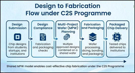
ChipIN Centre: National Enabler under the C2S Programme
The ChipIN Centre at C-DAC Bengaluru serves as one of India’s largest shared semiconductor design infrastructure facilities for academic institutions and start-ups. It provides comprehensive support across the entire chip design lifecycle, including access to commercial EDA tools, compute infrastructure, IP libraries, and technical mentorship.
Role of ChipIN Centre
1. Design Collection and Fabrication: Student chip designs from C2S institutions are collected and aggregated every three months and sent to Semiconductor Laboratory (SCL), Mohali, for fabrication using 180 nm technology.
2. Design Verification: The Centre verifies designs for fabrication readiness, supports iterative improvements, and aggregates approved designs onto shared wafers for cost-effective fabrication.
3. Fabrication and Delivery: SCL Mohali fabricates, packages, and returns chips to institutions, enabling students to validate designs on silicon.
4. Technical Support: The ChipIN Centre provides continuous centralised support, having addressed 4,855 support requests to date.
Key Outcomes of the C2S Programme
The Chips to Start-up Programme has delivered measurable outcomes across capacity building, infrastructure access, and hands-on design enablement:
1. ~1 lakh individuals from 400 organisations (300 academic institutions and 95 startups) utilised shared national EDA infrastructure
2. 175+ lakh hours of EDA tool usage recorded
3. 6 shared wafer runs conducted at SCL Mohali
4. 122 chip design submissions from 46 institutions
5. 56 student-designed chips successfully fabricated, packaged, and delivered
6. 265+ industry-led training sessions conducted
7. 75+ patents filed by participating institutions
8. 500+ IP cores, ASICs, and SoC designs under development across defence, telecom, automotive, consumer electronics, and industrial sectors
9. Deployment of centralised and distributed FPGA boards for prototyping and validation
10. Access to high-performance computing via the PARAM Utkarsh supercomputer
Institutional Framework Supporting the C2S Programme
India’s chip design ecosystem under C2S is supported by a coordinated institutional framework integrating policy direction, infrastructure enablement, and industry collaboration.
Ministry of Electronics and IT (MeitY)
MeitY provides overall policy direction, funding support, and programme oversight. Through initiatives such as C2S, it seeks to address structural gaps in India’s semiconductor ecosystem and enable domestic firms to move up the global value chain.
Centre for Development of Advanced Computing (C-DAC)
C-DAC operates the ChipIN Centre, providing shared access to EDA tools, high-performance computing, IP libraries, and technical mentoring. It manages design onboarding, verification, and fabrication coordination.
Semi-Conductor Laboratory (SCL), Mohali
SCL facilitates fabrication and packaging of academic chip designs under shared wafer runs, providing students with critical exposure to post-fabrication testing and validation. Together, these institutions ensure equitable access to national infrastructure, strengthen academia–industry linkages, and build a sustained pipeline of industry-ready chip designers.
Conclusion
Semiconductors have emerged as a strategic foundation for innovation, economic growth, and national security. Leadership in chip design and talent development is increasingly central to global technological competitiveness. The Chips to Start-up Programme represents a decisive step in India’s semiconductor journey. By combining large-scale skill development, hands-on design experience, and access to national infrastructure, the programme is empowering students, researchers, startups, and entrepreneurs to contribute meaningfully to indigenous chip design and innovation. These efforts are strengthening India’s talent base, advancing technological self-reliance, and positioning the country as a credible and competitive hub in the global semiconductor ecosystem.
Best ias coaching in delhi Best ias coaching in chandigarh
Prelims question:
Q. With reference to the Chips to Start-up (C2S) Programme, consider the following statements:
1. The C2S Programme is implemented by the Ministry of Electronics and Information Technology (MeitY) to build indigenous semiconductor chip design capacity.
2. Under the programme, student-designed chips are fabricated through shared wafer runs at the Semi-Conductor Laboratory (SCL), Mohali.
3. The programme exclusively focuses on undergraduate-level training and does not cover postgraduate or doctoral research.
4. The ChipIN Centre at C-DAC Bengaluru provides shared access to industry-grade Electronic Design Automation (EDA) tools.
Which of the statements given above are correct?
(a) 1, 2 and 4 only
(b) 1 and 3 only
(c) 2 and 4 only
(d) 1, 2, 3 and 4
Answer: A
Q. Semiconductors have emerged as a strategic pillar for economic growth, technological sovereignty, and national security. In this context, examine the objectives, institutional framework, and significance of the Chips to Start-up (C2S) Programme in strengthening India’s semiconductor chip design ecosystem.
(250 words)
- E-NAM and the Transformation of Agricultural Marketing in India - April 17, 2026
- Indian Railways: Journey from Steam Engines to a Modern Transport Backbone - April 16, 2026
- Mission Poshan 2.0: Strengthening India’s Nutrition Ecosystem - April 15, 2026
No Comments