


15 Jul Cabinet Approves Semicon 2.0: India’s Semiconductor Manufacturing Push
Subject Relevance — Where This Topic Fits
- GS Paper III — Indian Economy and issues relating to Planning, Mobilization of Resources, Growth, Development and Employment. | GS Paper III — Science and Technology- developments and their applications and effects in everyday life. Indigenization of technology and developing new technology. | GS Paper III — Infrastructure: Energy, Ports, Roads, Airports, Railways etc. | GS Paper II — Government Policies and Interventions for Development in various sectors and Issues arising out of their Design and Implementation.
- Prelims: Semicon India Program, Semiconductor Fab, ATMP/OSAT, Compound Semiconductors, Design Linked Incentive (DLI), Strategic Electronics, Clean Room Technology, 28nm node, Gallium Nitride, Silicon Carbide
- Essay: Technological Sovereignty as a Cornerstone of National Power and Economic Prosperity., The Role of Government Policy in Fostering Indigenous Innovation and Industrial Growth.
Quick Revision: Semicon 2.0 is India’s INR 1.27 lakh crore, six-pillar program aimed at achieving semiconductor self-reliance and global leadership in design, manufacturing, and R&D, crucial for economic growth and strategic autonomy.
Why is this in the news?
The Union Cabinet, chaired by Prime Minister Shri Narendra Modi, has recently approved ‘Semicon 2.0’, allocating a substantial budget of INR 1,27,500 crore. This approval signifies the government’s renewed and long-term commitment to establishing India as a prominent global hub for semiconductor design and manufacturing, building upon the momentum generated by the initial Semicon India Program (Semicon 1.0) and addressing the critical need for sustained policy support in this strategic sector.
Background
- The global semiconductor industry is a cornerstone of modern technology, underpinning everything from consumer electronics to critical infrastructure and defence systems.
- India, despite its strong IT services sector, has historically been heavily reliant on imports for semiconductor chips, creating significant vulnerabilities in its supply chain and national security.
- The COVID-19 pandemic exposed the fragility of global supply chains, leading to a severe semiconductor shortage that impacted various industries worldwide, highlighting the urgent need for diversification and indigenous manufacturing capabilities.
- The initial Semicon India Program (Semicon 1.0), launched with a financial outlay, aimed to kickstart the semiconductor ecosystem in India by attracting investments in manufacturing and design.
- Semicon 1.0 witnessed significant progress, with twelve manufacturing units approved, including silicon fabs, compound semiconductor fabs, and packaging units, demonstrating growing global confidence in India’s potential.
- The government’s vision is to move beyond being just a consumer of technology to becoming a key player in its production, fostering a robust ‘Atmanirbhar Bharat’ (self-reliant India) in critical technologies.
What is Semicon 2.0?
- Semicon 2.0 is the enhanced and expanded iteration of India’s national program for the development of a comprehensive semiconductor ecosystem, approved with an outlay of INR 1,27,500 crore.
- It aims to position India firmly on the global semiconductor map by fostering indigenous capabilities in design, manufacturing, and R&D.
- The program builds upon the initial successes of Semicon 1.0, which saw the approval of 12 manufacturing units and the commencement of commercial production by some key players.
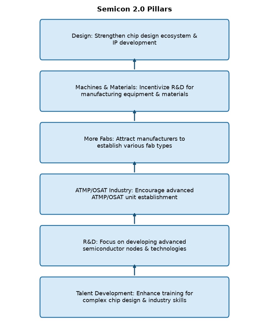
- It adopts a holistic, six-pillar strategy to create a robust semiconductor ecosystem, encompassing design, materials, manufacturing, packaging, R&D, and talent development.
- A key objective is to attract more global manufacturers to establish various types of fabs in India, including Silicon Fabs, Compound Semiconductor Fabs, Discrete Component Fabs, and Display Fabs.
- Semicon 2.0 seeks to strengthen India’s national security by reducing reliance on foreign supply chains for critical electronic components and promoting technological leadership in strategic sectors.
- It is designed to provide long-term policy support and incentives, ensuring the sustainable growth and competitiveness of India’s semiconductor industry.
Key Features
| Feature | Significance |
|---|---|
| Design Focus (Pillar 1) | Leverages early success with 105 startups, aiming to make India a major hub for IP, chip design, and system development, fostering indigenous innovation. |
| Machines & Materials (Pillar 2) | Incentivizes R&D and manufacturing of essential equipment, chemicals, and gases, building foundational support for the semiconductor industry and precision manufacturing. |
| Increased Fab Establishment (Pillar 3) | Attracts more manufacturers for diverse fabs (Silicon, Compound, Discrete, Display), boosting domestic production and reducing import dependence. |
| Strengthening ATMP/OSAT (Pillar 4) | Promotes India as an alternative location for advanced Assembly, Testing, Marking, and Packaging (ATMP) and Outsourced Semiconductor Assembly and Test (OSAT) units, enhancing value chain presence. |
| Advanced R&D (Pillar 5) | Focuses on developing more advanced process nodes (beyond 28nm-110nm) and cutting-edge technologies through collaboration with national and international R&D centers. |
| Talent Development (Pillar 6) | Expands training in complex chip design for 68,000+ students across 315 universities, involving industry in clean room and fab construction training, ensuring a skilled workforce. |
Why it Matters
Economic Growth and Diversification
- Fosters a high-tech manufacturing base, creating numerous direct and indirect employment opportunities in engineering, R&D, and skilled labour.
- Attracts significant foreign direct investment (FDI) and promotes domestic capital formation in a capital-intensive industry.
- Drives economic growth across various sectors, including consumer electronics, automotive, industrial electronics, and telecommunications, by ensuring a stable supply of critical components.
- Reduces India’s import bill for electronic components, improving its balance of payments and strengthening the rupee.
Strategic Autonomy and National Security
- Mitigates geopolitical risks associated with global supply chain disruptions and over-reliance on a few countries for critical components.
- Enhances India’s strategic autonomy by ensuring indigenous availability of semiconductors for defence, aerospace, and critical infrastructure applications.
- Positions India as a reliable and secure partner in the global technology supply chain, strengthening its geopolitical standing.
- Contributes to ‘Atmanirbhar Bharat’ by building self-sufficiency in a foundational technology, crucial for national resilience.
Technological Advancement and Innovation
- Stimulates cutting-edge research and development in materials science, quantum computing, AI, and advanced manufacturing processes.
- Fosters a culture of innovation and entrepreneurship, particularly in chip design and IP development, making India a hub for next-generation technologies.
- Develops a highly skilled workforce, capable of driving future technological advancements and maintaining India’s competitive edge.
- Facilitates the adoption of advanced manufacturing techniques and clean room technologies, raising overall industrial standards.
Challenges
1. High Capital Investment and Long Gestation Periods
- Semiconductor manufacturing (fabs) requires multi-billion dollar investments and takes several years to become operational and profitable.
- The substantial initial outlay and long return on investment can deter private players without robust government incentives and sustained support.
UPSC Link: GS Paper III — Mobilization of Resources
2. Technological Complexity and Rapid Obsolescence
- The semiconductor industry is characterized by extremely complex manufacturing processes and a rapid pace of technological change (Moore’s Law).
- Maintaining competitiveness requires continuous investment in R&D and upgrading to newer, more advanced process nodes, posing a significant challenge.
UPSC Link: GS Paper III — Science and Technology
3. Skilled Workforce and Talent Gap
- The industry demands a highly specialized workforce, including chip designers, process engineers, material scientists, and cleanroom technicians.
- Despite training efforts, a significant gap exists between the demand for such specialized talent and the available supply in India.
UPSC Link: GS Paper III — Human Resource Development
4. Infrastructure Requirements
- Fabs require uninterrupted power supply, vast quantities of ultra-pure water, and a highly stable and dust-free environment (cleanrooms).
- Developing and maintaining such world-class infrastructure across multiple locations in India presents a logistical and financial challenge.
UPSC Link: GS Paper III — Infrastructure
5. Global Competition and Geopolitics
- India faces intense competition from established semiconductor manufacturing hubs like Taiwan, South Korea, and the US, which have decades of experience and robust ecosystems.
- Geopolitical tensions and trade wars can influence investment decisions and access to critical technologies and intellectual property.
UPSC Link: GS Paper II — International Relations
Challenges — UPSC Perspective
| Issue | Concern |
|---|---|
| Capital Intensity | Multi-billion dollar investments required for fabs, long gestation periods, and high risk for private investors. |
| Technological Frontier | Keeping pace with rapid advancements (e.g., sub-7nm nodes) and avoiding technological obsolescence is challenging. |
| Ecosystem Maturity | Lack of a fully developed ancillary industry for equipment, chemicals, and gases compared to established hubs. |
| Water & Power | Huge demand for ultra-pure water and uninterrupted, high-quality power supply for fab operations. |
| IP & Licensing | Navigating complex intellectual property rights and licensing agreements in a highly proprietary industry. |
| Global Talent Pool | Attracting and retaining top global talent and expertise to build and operate advanced facilities in India. |
Government Initiatives — Must-Memorise for Prelims
- Design Linked Incentive (DLI) Scheme
- Productivity Linked Incentive (PLI) Scheme for Large Scale Electronics Manufacturing
- Scheme for Promotion of Manufacturing of Electronic Components and Semiconductors (SPECS)
- Modified Electronics Manufacturing Clusters (EMC 2.0) Scheme
- National Policy on Electronics (NPE)
- India Semiconductor Mission (ISM)
- Skill India Mission
- Make in India initiative
- National Research Foundation (NRF)
- Digital India Programme
Way Forward
- Sustained and Predictable Policy Support: Ensure long-term stability and predictability in policy incentives, tax benefits, and regulatory frameworks to attract and retain large-scale investments.
- Targeted Skill Development: Implement advanced, industry-specific training programs in collaboration with global leaders, focusing on niche skills like process engineering, cleanroom operations, and advanced chip design.
- Strengthening R&D Ecosystem: Foster strong linkages between academia, industry, and national research labs to drive innovation in advanced materials, process technologies, and next-generation chip architectures.
- Developing Ancillary Industries: Incentivize the development of a robust local supply chain for critical raw materials, chemicals, gases, and manufacturing equipment to reduce import dependence.
- Strategic International Collaborations: Forge partnerships with leading semiconductor nations and companies for technology transfer, joint ventures, and access to global markets and expertise.
- Infrastructure Enhancement: Prioritize the development of world-class infrastructure, including reliable power, ultra-pure water supply, and logistics, specifically tailored for semiconductor manufacturing zones.
- Ease of Doing Business: Streamline regulatory approvals, environmental clearances, and land acquisition processes to create an attractive and efficient investment climate.
- Focus on Niche Areas: While pursuing advanced fabs, also focus on niche areas like compound semiconductors, power electronics, and ATMP, where India can quickly build competitive advantages.
UPSC Value Addition
Keywords for Mains Answer-Writing
Semiconductor Ecosystem · Strategic Autonomy · Technological Sovereignty · Atmanirbhar Bharat · Global Supply Chain Resilience · High-Tech Manufacturing · Design Linked Incentive · Fab Manufacturing · ATMP/OSAT · Advanced Process Nodes · Skilled Workforce Development · Precision Manufacturing · Geopolitical Leverage · Digital Economy Enabler
Constitutional & Policy Linkages
- Article 19(1)(g): Right to practice any profession, or to carry on any occupation, trade or business (economic development)
- Article 38: State to secure a social order for the promotion of welfare of the people (economic justice, reducing disparities)
- Article 39(b) & (c): Distribution of material resources for common good, prevention of concentration of wealth (equitable industrial growth)
- Article 41: Right to work, to education and to public assistance in certain cases (skill development, employment generation)
- Article 43: Living wage, etc., for workers (fair labour practices in new industries)
- Article 51A(j): Strive towards excellence in all spheres of individual and collective activity (scientific temper, technological advancement)
- IT Act, 2000: Legal framework for electronic transactions and cyber security (digital infrastructure support)
Concept Flow
Global Semiconductor Shortage -> Exposed India’s Import Dependence → Semicon 1.0 Launch -> Initial Incentives & Investment Approvals → Growing Confidence & Progress -> Need for Sustained Support → Semicon 2.0 Approval (INR 1.27 Lakh Cr) -> Holistic 6-Pillar Strategy → Increased Fab & ATMP -> Boost to Domestic Manufacturing & Packaging → Design & R&D Focus -> Indigenous IP & Advanced Technology Development → Talent Development -> Skilled Workforce for Future Growth → Result: India as Global Semiconductor Hub -> Economic Growth & Strategic Autonomy
Prelims Practice Questions
Q1. Consider the following statements regarding Semicon 2.0:
1. It aims to establish India as a global hub for semiconductor design and manufacturing.
2. The program focuses solely on silicon fab manufacturing, excluding compound semiconductors.
3. Talent development and advanced R&D are among its six core pillars.
Which of the statements given above is/are correct?
- A. 1 only
- B. 1 and 3 only
- C. 2 and 3 only
- D. 1, 2 and 3
Answer: B. 1 and 3 only — Statement 1 is correct as Semicon 2.0’s primary goal is to establish India as a global semiconductor hub. Statement 2 is incorrect because Semicon 2.0 explicitly mentions attracting various types of fabs, including Silicon Fabs, Compound Semiconductor Fabs, Discrete Component Fabs, and Display Fabs. Statement 3 is correct as ‘Research & Development’ and ‘Talent Development’ are indeed two of the six pillars of Semicon 2.0.
Q2. Which of the following are key components of the semiconductor manufacturing ecosystem that Semicon 2.0 seeks to strengthen?
1. Design Linked Incentive (DLI) schemes.
2. Establishment of Assembly, Testing, Marking, and Packaging (ATMP) units.
3. Development of indigenous manufacturing capabilities for machines and materials.
4. Focus on advanced process nodes beyond 28nm.
Select the correct answer using the code given below:
- A. 1 and 2 only
- B. 2, 3 and 4 only
- C. 1, 3 and 4 only
- D. 1, 2, 3 and 4
Answer: D. 1, 2, 3 and 4 — All four statements are correct. Semicon 2.0 builds upon DLI schemes (implied by design focus), explicitly aims to strengthen ATMP/OSAT industry, incentivizes manufacturing of machines and materials, and focuses on developing more advanced nodes and technologies beyond the initial 28nm-110nm journey.
Mains Practice Question
✍ Discuss the strategic imperatives behind India’s ambitious ‘Semicon 2.0’ program. Evaluate the potential benefits and significant challenges in establishing a robust domestic semiconductor ecosystem, and suggest a comprehensive roadmap for its successful implementation. (250 words)
Approach: Begin by introducing Semicon 2.0 as a critical national initiative for technological sovereignty and economic growth. Detail the strategic imperatives, such as reducing import dependence, enhancing national security, and leveraging India’s digital economy. Subsequently, elaborate on the potential benefits, including job creation, FDI attraction, and fostering innovation. Concurrently, critically analyze the formidable challenges like high capital intensity, technological obsolescence, infrastructure demands, and the skilled talent gap. Conclude by outlining a comprehensive roadmap that includes sustained policy support, targeted skill development, R&D ecosystem strengthening, international collaborations, and efficient infrastructure development, ensuring a holistic and sustainable approach.
Source: PIB (Press Information Bureau)

- Odisha vs Andhra Pradesh: Supreme Court Contempt Over Kotia Polls - October 24, 2026
- आरबीआई द्वारा 91, 182 और 364 दिनीय ट्रेजरी बिलों की नीलामी: प्रमुख तथ्य - October 24, 2026
- Inflation’s Second-Round Effects: RBI Policy & Economic Impact Analysis - October 24, 2026

No Comments