


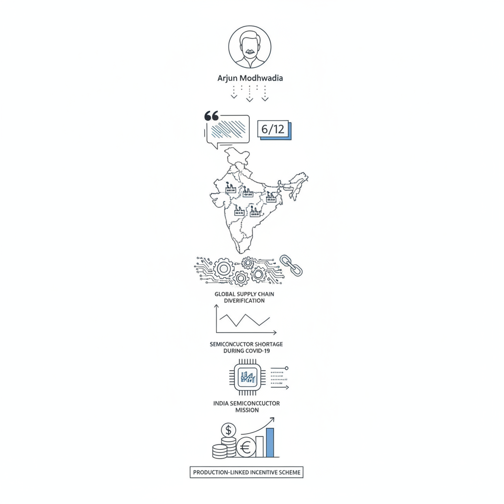
14 Sep Gujarat to host 6 of India’s 12 semiconductor facilities: Key UPSC insights
✎ Semiconductor fabs are capital-intensive, clean-room-based facilities essential for domestic chip manufacturing, and Gujarat’s strategic infrastructure positions it as a key player in India’s semiconductor mission.
Subject Relevance — Where This Topic Fits
- GS Paper III — Science and Technology | GS Paper III — Industrial Policy and Infrastructure | GS Paper III — Government Budgeting and Financial Incentives
- Prelims: Semiconductor Mission, Production-Linked Incentive (PLI) Scheme, Semiconductor Fabrication Unit (FAB), Dholera SIR, Data Centre Policy
- Essay: Technological Self-Reliance: India’s Semiconductor Vision, Balancing Environmental Sustainability and Industrial Growth
Quick Revision: Semiconductor fabs are capital-intensive, clean-room-based facilities essential for domestic chip manufacturing, and Gujarat’s strategic infrastructure positions it as a key player in India’s semiconductor mission.
Why is this in the news?
The statement by Gujarat’s Minister for Science and Technology highlights the state’s pivotal role in India’s semiconductor manufacturing expansion, with six of the twelve proposed facilities located in Gujarat. This development underscores the strategic importance of semiconductor ecosystems in India’s industrial policy, particularly in the context of global supply chain diversification and domestic capacity building.
Background
- The global semiconductor shortage during the COVID-19 pandemic exposed vulnerabilities in supply chains, prompting countries to prioritise domestic semiconductor manufacturing.
- India launched the Semiconductor Mission in December 2021 with an outlay of ₹76,000 crore to develop a robust semiconductor and display manufacturing ecosystem.
- The Production-Linked Incentive (PLI) Scheme for Large Scale Electronics Manufacturing and the Scheme for Promotion of Manufacturing of Electronic Components and Semiconductors (SPECS) provide financial incentives for semiconductor fabrication units.
- Gujarat’s strategic advantages include robust logistics infrastructure (ports, highways, airports), high-quality power infrastructure, and proximity to major consumption and manufacturing centres.
- The Dholera Special Investment Region (SIR) is a key infrastructure project aimed at creating a plug-and-play industrial ecosystem, including semiconductor manufacturing.
What are Semiconductor Manufacturing Facilities?
- Semiconductor manufacturing facilities, or fabs, are industrial units engaged in the fabrication of integrated circuits (ICs) and microchips, which are critical components for electronic devices.
- Semiconductor fabs require highly specialised infrastructure, including clean rooms, advanced manufacturing equipment, and uninterrupted high-quality power supply.
- The semiconductor industry is capital-intensive, with fabrication units requiring investments in the range of billions of dollars for a single facility.
- India’s semiconductor mission aims to reduce import dependence by developing domestic manufacturing capabilities, aligning with the broader goal of ‘Atmanirbhar Bharat’ (self-reliant India).
- Semiconductor fabs are classified into different types, including fabrication units (FABs), assembly, testing, marking, and packaging (ATMP) units, and display fabrication units.
- The establishment of semiconductor fabs involves multi-stakeholder collaboration, including central and state governments, private investors, and international technology partners.
- Gujarat’s semiconductor facilities are part of a broader strategy to position India as a global hub for high-tech manufacturing, leveraging its industrial corridors and skilled workforce.
Key Features
| Feature | Significance |
|---|---|
| Semiconductor Manufacturing Facilities | Gujarat will host six of India’s twelve semiconductor facilities, with a combined investment exceeding ₹1.28 lakh crore, positioning the state as a critical node in India’s semiconductor ecosystem. |
| High-Quality Power Infrastructure | Reliable and resilient power supply is essential for semiconductor fabrication, where uninterrupted electricity is non-negotiable for precision manufacturing processes. |
| Plug-and-Play Industrial Corridors | Dholera and Sanand offer pre-developed infrastructure with integrated logistics, reducing setup time and operational costs for semiconductor firms. |
| Data Centre Policy 2026-29 | Targets 7.5 GW of data centre capacity, aiming to attract hyperscale, AI-ready facilities, and leveraging Gujarat’s energy resilience for green-powered operations. |
| Skill Development Initiatives | Training programmes in India and abroad for local youth, including tribal communities, to build a skilled workforce for high-tech industries like semiconductors. |
| Proximity to Consumption Hubs | Strategic location near major manufacturing and consumption centres reduces logistics costs and enhances supply chain efficiency for semiconductor and electronics industries. |
Why it Matters
Economic
- Semiconductor manufacturing is a high-value, high-employment industry; Gujarat’s initiative could generate thousands of direct and indirect jobs, including in R&D and ancillary sectors.
- Attracts foreign direct investment (FDI) and fosters technology transfer, enhancing India’s self-reliance in critical electronics components.
- Boosts ancillary industries such as precision engineering, chemicals, and logistics, creating a multiplier effect on state GDP.
- Positions Gujarat as a global semiconductor hub, competing with established centres in East Asia and the United States.
Strategic
- Reduces India’s dependence on semiconductor imports, addressing supply chain vulnerabilities exposed during geopolitical disruptions.
- Supports India’s ‘Atmanirbhar Bharat’ vision by building domestic capacity in a sector dominated by a few global players.
- Enhances national security by ensuring a stable supply of semiconductors for defence, space, and critical infrastructure applications.
Technological
- Facilitates the development of a semiconductor design and fabrication ecosystem, bridging the gap between R&D and commercial production.
- Encourages innovation in adjacent sectors like AI, IoT, and 5G, where semiconductor demand is rapidly growing.
- Promotes adoption of advanced manufacturing techniques, including automation and Industry 4.0 practices, in Gujarat’s industrial landscape.
Environmental
- Gujarat’s focus on green energy for data centres aligns with India’s climate commitments and reduces the carbon footprint of high-energy industries.
- Integration of renewable energy sources in semiconductor parks can set a precedent for sustainable industrial development.
Challenges
1. Ecosystem Development
- Creating a robust ecosystem requires coordination among multiple stakeholders, including central and state governments, private investors, and academic institutions.
- The semiconductor industry demands a highly skilled workforce; rapid upskilling is essential to meet industry standards.
- Building trust among global investors is critical, as semiconductor fabrication involves long gestation periods and high capital risks.
UPSC Link: GS3: Industrial Policy & Ease of Doing Business
2. Infrastructure Bottlenecks
- Despite Gujarat’s strengths, ensuring uninterrupted power supply, water availability, and waste management at scale remains a challenge.
- Logistics and connectivity, while strong, must be continuously upgraded to handle the volume and precision requirements of semiconductor supply chains.
UPSC Link: GS3: Infrastructure & Logistics
3. Global Competition
- India competes with established semiconductor hubs like Taiwan, South Korea, and the US, which offer mature ecosystems and incentives.
- Geopolitical tensions and trade restrictions (e.g., export controls on advanced semiconductor equipment) can disrupt supply chains.
UPSC Link: GS2: International Relations & Trade
4. Regulatory and Bureaucratic Hurdles
- Land acquisition, environmental clearances, and compliance with multiple regulations can delay project timelines.
- Streamlining approvals for high-tech industries without compromising environmental or labour standards is a delicate balance.
UPSC Link: GS2: Governance & E-Governance
5. Skill Gap and Retention
- Retaining talent trained abroad or in premier Indian institutions is challenging, as global firms compete for the same pool of skilled professionals.
- Vocational training programmes must align with industry needs to avoid mismatches in skill supply and demand.
UPSC Link: GS3: Education & Skill Development
Challenges — UPSC Perspective
| Issue | Concern |
|---|---|
| High Capital Expenditure | Semiconductor fabrication requires billions in investment, with long payback periods, deterring risk-averse investors. |
| Technology Transfer Restrictions | Global semiconductor firms may hesitate to share proprietary technology due to geopolitical and competitive reasons. |
| Water and Energy Intensity | Semiconductor manufacturing is highly resource-intensive; ensuring sustainable water and energy supply is critical. |
| Supply Chain Dependencies | India relies on imports for key inputs like silicon wafers and advanced machinery, creating vulnerabilities. |
| Environmental Regulations | Balancing rapid industrialisation with stringent environmental norms (e.g., EIA 2006) poses compliance challenges. |
| Talent Shortage | Limited number of institutions offering semiconductor-specific courses; industry-academia collaboration is nascent. |
Government Initiatives — Must-Memorise for Prelims
- India Semiconductor Mission (ISM)
Way Forward
- Accelerate the establishment of Gujarat’s semiconductor parks by fast-tracking land acquisition and environmental clearances under the ISM framework.
- Expand skill development programmes in collaboration with IITs, NITs, and industry partners to address the talent shortage in semiconductor fabrication.
- Strengthen Gujarat’s power infrastructure by integrating renewable energy sources and ensuring 24/7 uninterrupted supply to high-tech industries.
- Develop a state-level semiconductor policy with incentives for R&D, startups, and MSMEs to foster innovation and ancillary industry growth.
- Enhance logistics connectivity by upgrading ports, highways, and airports, with a focus on cold-chain and precision logistics for semiconductor components.
- Establish a dedicated semiconductor research centre in Gujarat to bridge the gap between academic research and industrial application.
- Promote public-private partnerships (PPPs) for shared infrastructure like testing labs, prototyping facilities, and waste management systems.
- Monitor and address environmental concerns proactively through regular audits and adoption of green manufacturing practices.
UPSC Value Addition
Keywords for Mains Answer-Writing
Semiconductor manufacturing policy · India Semiconductor Mission · Gujarat industrial policy · semiconductor fabrication facility · Viksit Bharat Semicon 2026 · data centre policy · high-tech manufacturing ecosystem · plurilateral industrial corridors · semiconductor supply chain · green energy data centres
Concept Flow
Government of India launches the India Semiconductor Mission (ISM) to reduce import dependence and boost domestic semiconductor manufacturing. → Gujarat leverages its strategic advantages—logistics, power infrastructure, and proximity to markets—to attract semiconductor firms under the ISM. → Semiconductor firms evaluate Gujarat’s ecosystem, including incentives, skill availability, and infrastructure, before committing investments. → State government signs MoUs with anchor companies (e.g., Tata Electronics, PSMC) and approves additional facilities (e.g., Suchi Semicon, Crystal Matrix). → Anchor companies establish fabrication units, while ancillary industries and skill development programmes are set up to support the ecosystem. → Semiconductor production begins, integrating with Gujarat’s data centre policy to create a high-tech industrial cluster with green energy focus. → Gujarat emerges as a global semiconductor hub, contributing to India’s self-reliance, economic growth, and technological sovereignty.
Prelims Practice Questions
Q1. Consider the following statements regarding the India Semiconductor Mission (ISM):
1. The ISM is a central sector scheme under the Ministry of Electronics and Information Technology.
2. The ISM aims to build a resilient semiconductor and display ecosystem in India.
3. The ISM provides 50% fiscal support for setting up semiconductor fabrication facilities in India.
How many of the above statements are correct?
- Only one
- Only two
- Only three
- None
Answer: Only three — Statements 1 and 2 are correct. Statement 3 is incorrect as the fiscal support under ISM for semiconductor fabrication facilities is up to 50% of the project cost, but this is subject to caps and conditions.
Q2. Assertion (A): Gujarat’s semiconductor policy focuses on leveraging its port-led logistics infrastructure to attract high-tech manufacturing.
Reason (R): The state’s proximity to major consumption centres and robust power infrastructure are critical enablers for semiconductor manufacturing.
Options:
A. Both A and R are true, and R is the correct explanation of A.
B. Both A and R are true, but R is NOT the correct explanation of A.
C. A is true, but R is false.
D. A is false, but R is true.
Answer: ? — Both the assertion and reason are true, and the reason correctly explains the assertion. Gujarat’s port-led logistics and power infrastructure are key factors in attracting semiconductor investments.
Q3. Match the following semiconductor manufacturing facilities with their respective locations in Gujarat:
Column I
1. Tata Electronics semiconductor fabrication facility
2. Suchi Semicon’s facility
3. Crystal Matrix’s facility
4. CG Semi facility
Column II
A. Sanand
B. Dholera
C. Surat
Options:
1-A, 2-C, 3-B, 4-A
1-B, 2-C, 3-B, 4-A
1-A, 2-B, 3-C, 4-A
1-B, 2-A, 3-C, 4-B
Answer: ? — Tata Electronics’ facility is in Dholera (1-B), Suchi Semicon’s facility is in Surat (2-C), Crystal Matrix’s facility is in Dholera (3-B), and CG Semi’s facility is in Sanand (4-A).
Mains Practice Question
✍ Critically examine the role of state-level industrial policies in fostering high-tech manufacturing ecosystems, with special reference to Gujarat’s semiconductor and data centre initiatives. Also, analyse the challenges in creating such ecosystems and the measures required to sustain them. (15 Marks)
Approach: MODEL-ANSWER SKELETON:
1. Introduction (2 marks)
– Define high-tech manufacturing ecosystems and their significance for ‘Viksit Bharat’ and self-reliance (Atmanirbhar Bharat).
– Briefly introduce Gujarat’s initiatives: Semiconductor Policy 2026-29, Viksit Gujarat Data Centre Policy 2026-29, and plurilateral industrial corridors (Dholera, Sanand).
2. Gujarat’s Policy Framework and Enablers (4 marks)
– Semiconductor Policy: fiscal incentives (up to 50% of project cost), land allotment, single-window clearance, and skill development (e.g., training in Taiwan, Chennai, Bengaluru).
– Data Centre Policy: 7.5 GW target, green energy focus, and AI-ready infrastructure.
– Logistics and infrastructure: ports (e.g., Mundra), highways (e.g., Delhi-Mumbai Industrial Corridor), airports, and resilient power supply.
– Institutional mechanisms: Gujarat Industrial Development Corporation (GIDC), Gujarat Maritime Board (GMB), and Gujarat Energy Research and Management Institute (GERMI).
3. Challenges in Ecosystem Creation (4 marks)
– High capital intensity and long gestation periods in semiconductor manufacturing.
– Skill gaps and brain-drain reversal: need for continuous upskilling and retention of returning executives.
– Supply chain vulnerabilities: dependence on imported raw materials (e.g., silicon wafers) and equipment.
– Regulatory hurdles: environmental clearances, land acquisition, and inter-state coordination.
– Global competition: attracting anchor investors amid subsidies offered by other nations (e.g., US CHIPS Act, EU Chips Act).
4. Measures to Sustain Ecosystems (3 marks)
– Strengthening R&D linkages with institutions (e.g., IITs, IISc) and industry-academia collaborations.
– Developing ancillary industries: precision engineering, chemicals, and packaging.
– Policy stability and predictability: long-term fiscal incentives and ease of doing business improvements.
– Public-private partnerships (PPPs) for shared infrastructure (e.g., common testing labs, power substations).
– Focus on sustainability: integration of green energy (e.g., solar, wind) and circular economy principles.
5. Comparative Perspective (2 marks)
– Contrast Gujarat’s approach with other states (e.g., Tamil Nadu’s electronics manufacturing, Karnataka’s aerospace policy).
– Highlight the role of the India Semiconductor Mission (ISM) in coordinating centre-state efforts.
Conclusion (2 marks)
– Summarise the transformative potential of state-led high-tech ecosystems for India’s industrialisation.
– Emphasise the need for a balanced approach: incentives must be calibrated to avoid fiscal strain while ensuring global competitiveness.
Source: The Indian Express
Gujarat PCS (GPSC) — State PCS Practice
Prelims: According to the recent interview of Arjun Modhwadia, how many of India’s 12 proposed semiconductor facilities are expected to be established in Gujarat?
- 3
- 6
- 9
- 12
Answer: 6 — Arjun Modhwadia stated that six of India’s 12 semiconductor facilities will be set up in Gujarat.
Mains: Discuss the strategic significance of Gujarat’s emergence as a major hub for semiconductor manufacturing in India. Examine the potential economic, technological, and employment-related impacts on the state.
Generated by AanyaAi for educational purpose.
Related guides on our sites
- How to prepare for GS paper 1 for UPSC CSE mains exam
- Best UPSC coaching for IFOS exam
- Best mentorship programme for upsc
- UPSC+BA degree

- Gujarat to host 6 of India’s 12 semiconductor facilities: Key UPSC insights - September 14, 2026
- डब्ल्यूपीआई मुद्रास्फीति अगस्त में बढ़कर 9.92% हुई: मुख्य कारण क्या हैं? - September 14, 2026
- WPI Inflation Hits 9.92% in August: Key Reasons & UPSC Implications - September 14, 2026
No Comments