


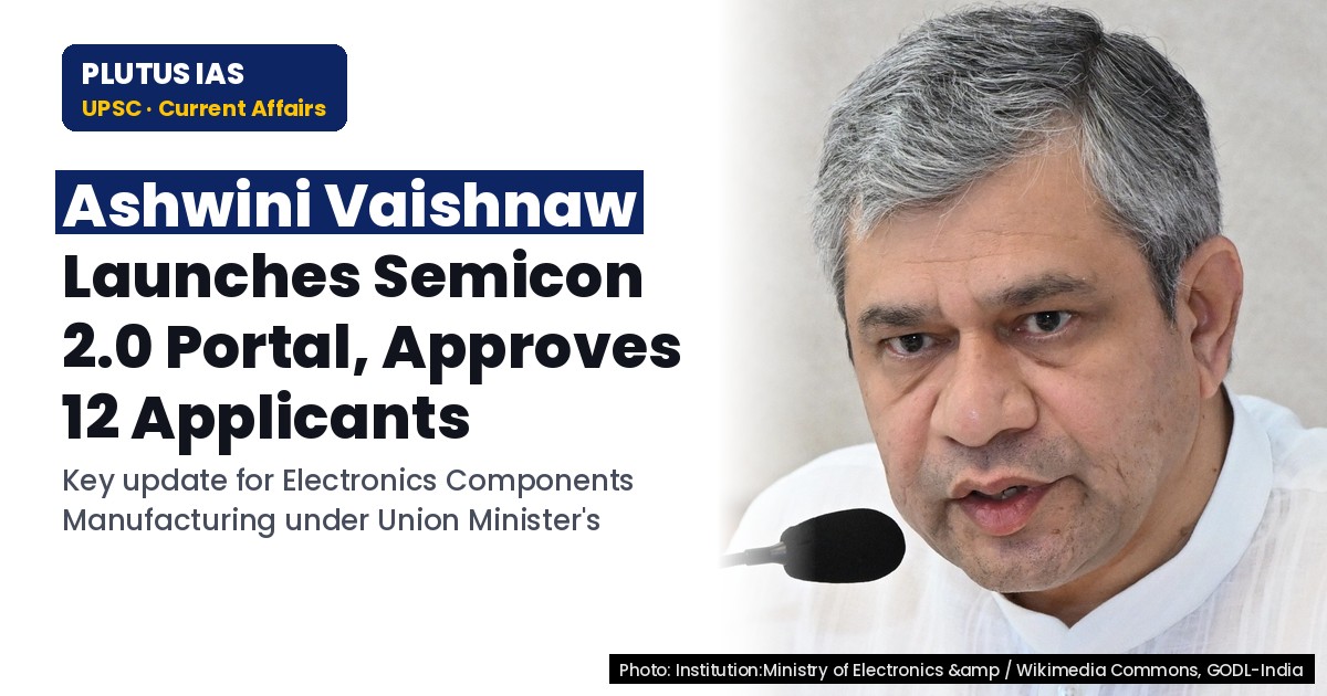
06 Nov Semicon 2.0 Web Portal Launched; 12 Applicants Approved
✎ Semicon 2.0 and SPECS are pivotal government initiatives aimed at fostering domestic semiconductor and electronics manufacturing by providing financial incentives and streamlining processes, thereby enhancing India's…
Subject Relevance — Where This Topic Fits
- GS Paper III — Economy — Industrial Policy, Infrastructure, Investment Models | GS Paper III — Science and Technology — Indigenization of Technology, Development of New Technologies
- Prelims: Semicon 2.0 Web Application Portal, Electronics Components Manufacturing Scheme (SPECS), Semiconductor manufacturing, Electronics manufacturing, Production Linked Incentive (PLI) Schemes, Make in India, Digital India, Ministry of Electronics and Information Technology (MeitY)
- Essay: The role of government policies in fostering a robust domestic manufacturing ecosystem., India’s journey towards technological self-reliance and global competitiveness in critical sectors.
Quick Revision: Semicon 2.0 and SPECS are pivotal government initiatives aimed at fostering domestic semiconductor and electronics manufacturing by providing financial incentives and streamlining processes, thereby enhancing India’s self-reliance and global competitiveness in these critical sectors.
Why is this in the news?
The Union Minister for Railways, Communications, and Electronics & Information Technology, Mr. Ashwini Vaishnaw, recently launched the Semicon 2.0 Web Application Portal. Concurrently, the Minister announced the approval of 12 applicants under the Scheme for Promotion of Manufacturing of Electronic Components and Semiconductors (SPECS), signifying a concerted governmental push to bolster domestic electronics and semiconductor manufacturing capabilities.
Background
- India’s electronics manufacturing sector has witnessed significant growth, driven by initiatives such as ‘Make in India’ and ‘Digital India’, aiming to transform the nation into a global manufacturing hub.
- The semiconductor industry is a foundational element for modern electronics, with its components being critical for a wide array of products, from consumer electronics to strategic defence equipment.
- Historically, India has been largely dependent on imports for semiconductors and high-end electronic components, leading to vulnerabilities in supply chains and economic outflow.
- Recognizing the strategic importance of this sector, the Government of India has introduced several schemes to incentivize domestic manufacturing, attract investments, and build a resilient supply chain.
- The global semiconductor shortage experienced in recent years underscored the imperative for nations to develop indigenous manufacturing capacities to ensure economic and national security.
- The overarching goal of these initiatives is to reduce import dependence, create employment opportunities, and establish India as a significant player in the global electronics and semiconductor value chain.
What are Semicon 2.0 and the Scheme for Promotion of Manufacturing of Electronic Components and Semiconductors (SPECS)?
- Semicon 2.0 Web Application Portal is an online platform designed to streamline the application and approval processes for various schemes aimed at promoting semiconductor and electronics manufacturing in India.
- It serves as a single-window interface for applicants, facilitating transparency, efficiency, and ease of doing business for companies seeking to invest in the sector.
- The Scheme for Promotion of Manufacturing of Electronic Components and Semiconductors (SPECS) was notified on April 1, 2020, by the Ministry of Electronics and Information Technology (MeitY).
- SPECS aims to offset the disability of domestic manufacturing of electronic components and semiconductors, thereby strengthening the electronics manufacturing ecosystem in the country.
- Under SPECS, a financial incentive of 25% of the capital expenditure is provided for the manufacturing of identified electronic components, sub-assemblies, and semiconductor devices.
- The scheme covers a wide range of electronic components, including those used in mobile phones, consumer electronics, industrial electronics, and automotive electronics, among others.
- The total outlay for the SPECS scheme is ₹3,285 crore.
- The scheme is crucial for attracting large-scale investments in the manufacturing of electronic components and semiconductors, which are essential for achieving the vision of a $1 trillion digital economy.
Key Features
| Feature | Significance |
|---|---|
| Semicon 2.0 Web Application Portal | Facilitates a streamlined application process for schemes promoting semiconductor and electronics manufacturing, enhancing ease of doing business and transparency. |
| 12 Approved Applicants | Indicates tangible progress in incentivizing domestic electronics component manufacturing, contributing to self-reliance and reducing import dependence. |
| Electronics Components Manufacturing Scheme (ECMS) | Aims to boost the production of electronic components, sub-assemblies, and capital goods, crucial for the broader electronics ecosystem. |
| Union Minister Ashwini Vaishnaw’s Announcement | Highlights the government’s continued commitment and strategic focus on developing India’s semiconductor and electronics manufacturing capabilities. |
Why it Matters
Economic Significance
- Fosters domestic value addition in electronics manufacturing, reducing reliance on imports and strengthening the balance of payments.
- Generates employment opportunities across the manufacturing value chain, from design to assembly and testing.
- Attracts foreign direct investment (FDI) into the high-technology manufacturing sector, promoting technology transfer and skill development.
Strategic Significance
- Enhances national security by reducing dependence on foreign sources for critical electronic components, particularly in strategic sectors.
- Positions India as a significant player in the global electronics supply chain, contributing to geopolitical influence and resilience.
- Supports the development of indigenous capabilities in cutting-edge technologies, crucial for future economic and technological sovereignty.
Technological Significance
- Accelerates research and development (R&D) in semiconductor design and manufacturing, fostering innovation within the country.
- Facilitates the adoption of advanced manufacturing processes and technologies, elevating India’s industrial capabilities.
- Enables the growth of ancillary industries and a robust ecosystem for electronics, including design, testing, and packaging.
Challenges
1. High Capital Investment
- Semiconductor fabrication units (fabs) require enormous upfront capital, posing a significant barrier to entry for new players.
- The long gestation period for returns on investment in semiconductor manufacturing can deter private sector participation without substantial government support.
UPSC Link: Economy: Industrial Policy
2. Technological Complexity and Rapid Obsolescence
- The semiconductor industry is characterized by extremely complex manufacturing processes and rapid technological advancements.
- Maintaining competitiveness requires continuous investment in R&D and upgrading facilities, which is a substantial challenge for developing nations.
UPSC Link: Science & Tech: IT & Computers
3. Skilled Manpower Shortage
- There is a global shortage of highly skilled engineers and technicians specializing in semiconductor design, fabrication, and packaging.
- Developing a robust talent pool requires significant investment in specialized education and training programs, with a long lead time.
UPSC Link: Human Resources: Skill Development
4. Global Supply Chain Vulnerabilities
- The semiconductor supply chain is highly globalized and susceptible to geopolitical tensions, natural disasters, and trade disputes.
- Building a resilient domestic supply chain requires extensive international collaboration and strategic partnerships.
UPSC Link: Economy: Globalisation
Challenges — UPSC Perspective
| Issue | Concern |
|---|---|
| Infrastructure Deficiencies | Reliable power supply, clean water, and specialized logistics are critical for semiconductor manufacturing, often lacking in sufficient quality and quantity. |
| Policy Consistency and Longevity | Long-term investments require stable and predictable policy frameworks that transcend political cycles to build investor confidence. |
| Intellectual Property Rights (IPR) | Ensuring robust IPR protection is crucial for attracting global technology leaders and fostering indigenous innovation in a high-tech sector. |
| Environmental Regulations | Semiconductor manufacturing is resource-intensive and generates specific waste; balancing industrial growth with stringent environmental norms is a challenge. |
Government Initiatives — Must-Memorise for Prelims
- Programme for Development of Semiconductors and Display Manufacturing Ecosystem in India
Way Forward
- Prioritize investment in R&D and innovation to develop indigenous capabilities in semiconductor design and advanced materials.
- Establish specialized educational institutions and skill development programs to create a skilled workforce for the semiconductor industry.
- Offer attractive fiscal incentives and subsidies to mitigate high capital costs and encourage both domestic and foreign investment.
- Develop a robust and reliable infrastructure, including uninterrupted power, water, and logistics, essential for high-tech manufacturing.
- Foster international collaborations and strategic partnerships to access advanced technology, expertise, and global markets.
- Implement a stable and long-term policy framework with clear objectives and consistent support to ensure investor confidence.
- Promote a ‘fabless’ model initially, focusing on design and intellectual property, before scaling up to full-scale fabrication.
UPSC Value Addition
Keywords for Mains Answer-Writing
Semiconductor manufacturing · Electronics components · Production Linked Incentive (PLI) · Make in India · Atmanirbhar Bharat · Digital India · Strategic sectors · Supply chain resilience · Economic growth · Technological self-reliance · Skill development · Foreign Direct Investment (FDI)
Concept Flow
Government announces Electronics Components Manufacturing Scheme (ECMS) → Semicon 2.0 Web Application Portal launched for scheme applications → Industry applicants submit proposals for electronics component manufacturing → Government approves 12 applicants under the scheme → Approved projects receive incentives and begin manufacturing → Domestic production of electronic components increases → India’s self-reliance in electronics manufacturing strengthens
Prelims Practice Questions
Q1. Consider the following statements regarding India’s semiconductor ecosystem initiatives:
1. The Semicon India Programme aims to provide financial support for semiconductor and display manufacturing units.
2. The Production Linked Incentive (PLI) scheme for Large Scale Electronics Manufacturing includes incentives for IT hardware and telecom products.
3. The Electronics Components Manufacturing Scheme (ECMS) primarily focuses on promoting the domestic manufacturing of electronic components and semiconductors.
How many of the above statements are correct?
- Only one
- Only two
- All three
- None
Answer: All three — Statement 1 is correct: The Semicon India Programme offers financial incentives to attract investments in semiconductor and display manufacturing. Statement 2 is correct: The PLI scheme for Large Scale Electronics Manufacturing covers various electronic products, including IT hardware and telecom equipment, to boost domestic production and exports. Statement 3 is correct: The Electronics Components Manufacturing Scheme (ECMS) is specifically designed to encourage the indigenous manufacturing of electronic components and semiconductors, thereby reducing import dependence and strengthening the domestic supply chain.
Q2. Which of the following is NOT a primary objective of government initiatives aimed at boosting semiconductor manufacturing in India?
- Achieving self-reliance in critical electronic components.
- Attracting global semiconductor giants to establish manufacturing units.
- Reducing India’s dependence on imported crude oil.
- Creating a skilled workforce for advanced technology sectors.
Answer: Reducing India’s dependence on imported crude oil. — Reducing India’s dependence on imported crude oil is primarily an objective of energy policy, not directly related to semiconductor manufacturing initiatives. The other options are direct objectives of such initiatives.
Mains Practice Question
✍ Examine the strategic importance of developing a robust domestic semiconductor manufacturing ecosystem for India’s economic and national security. Discuss the key policy initiatives undertaken by the government in this regard and evaluate their potential impact. (15 Marks)
Approach: MODEL-ANSWER SKELETON:
1. Introduction: Briefly define semiconductors and their pervasive role in modern technology.
2. Strategic Importance (Economic):
a. Reduced import dependence and foreign exchange savings.
b. Creation of high-value jobs and skill development.
c. Boost to allied industries (e.g., automotive, consumer electronics, IT).
d. Enhanced competitiveness in global digital economy.
e. Attracting Foreign Direct Investment (FDI).
3. Strategic Importance (National Security):
a. Supply chain resilience and mitigation of geopolitical risks.
b. Protection against cyber threats and espionage.
c. Indigenous development of critical defense and space technologies.
d. Data sovereignty and control over sensitive infrastructure.
4. Key Policy Initiatives:
a. Semicon India Programme (financial incentives for fabs, ATMP, display units).
b. Production Linked Incentive (PLI) schemes for Large Scale Electronics Manufacturing and IT Hardware.
c. Electronics Components Manufacturing Scheme (ECMS) / Scheme for Promotion of Manufacturing of Electronic Components and Semiconductors (SPECS).
d. Design Linked Incentive (DLI) Scheme.
e. Development of a skilled talent pool (e.g., India Semiconductor Mission).
5. Potential Impact:
a. Increased domestic value addition.
b. Diversification of global supply chains.
c. Emergence of India as a global manufacturing hub.
d. Enhanced technological self-reliance (Atmanirbhar Bharat).
e. Challenges: High capital investment, technological complexity, long gestation periods, need for sustained policy support.
6. Conclusion: Summarize the long-term benefits and reiterate the necessity of continued governmental and private sector collaboration.
Source: PIB (Press Information Bureau)
Generated by AanyaAi for educational purpose.
Related guides on our sites
- Best PSIR optional coaching for upsc
- Best PSIR optional teacher for upsc
- Best teacher of PSIR optional for upsc
- Best PSIR optional coaching in delhi for UPSC

- Semicon 2.0 Web Portal Launched; 12 Applicants Approved - November 6, 2026
- झारखंड HC: भाइयों की खरीदी जमीन में बहन का हिस्सा नहीं - November 6, 2026
- DSIR’s Special Campaign 6: 100% Target Achievement & Best Practices - November 6, 2026

No Comments