Designing the Future: India’s Semiconductor Ambitions and the Strategic Role of the Design Linked Incentive (DLI) Scheme

Designing the Future: India’s Semiconductor Ambitions and the Strategic Role of the Design Linked Incentive (DLI) Scheme

This article covers “Daily Current Affairs” and From  Designing the Future: India’s Semiconductor Ambitions and the Strategic Role of the Design Linked Incentive (DLI) Scheme

SYLLABUS MAPPING  

GS-3- Science & Technology- Designing the Future: India’s Semiconductor Ambitions and the Strategic Role of the Design Linked Incentive (DLI) Scheme

FOR PRELIMS

What is the Design Linked Incentive (DLI) Scheme?

FOR MAINS

What challenges does India face in commercialising indigenous semiconductor designs?

Why in the News?

Semiconductors are critical enablers of the digital economy, supporting sectors such as healthcare, telecommunications, defence, space, AI, and digital public infrastructure. With rapid digitalisation and AI-driven growth, global demand for chips is rising sharply, even as production and advanced design remain concentrated in a few countries, making supply chains fragile and geopolitically vulnerable. Against this backdrop, India has strengthened its semiconductor strategy under the Semicon India Programme and the India Semiconductor Mission (ISM). The Design Linked Incentive (DLI) Scheme has gained prominence for focusing on fabless chip design and intellectual property creation, the most value-intensive segment of the semiconductor value chain. By boosting indigenous design capabilities, India aims to reduce import dependence, enhance supply-chain resilience, and advance technological sovereignty.

Semiconductors as Strategic Infrastructure: Global and Indian Context

Global Supply Chain Vulnerabilities
1. Over 75% of advanced semiconductor manufacturing is concentrated in East Asia.
2. Geopolitical tensions, export controls, pandemics, and natural disasters have exposed the fragility of “just-in-time” semiconductor supply chains.
3. Countries are now prioritizing friend-shoring and diversification, creating strategic space for India.
India’s Opportunity
1. Rapid growth in electronics manufacturing, digital public infrastructure (DPI), EVs, defence electronics, and telecom networks.
2. Large domestic market combined with geopolitical trust.
3. Strong IT and embedded-systems talent base.
4. Policy clarity through long-term incentive frameworks.

Why Fabless Chip Design is the Core of Semiconductor Power

In the semiconductor value chain, fabless design companies capture the highest strategic and economic value:
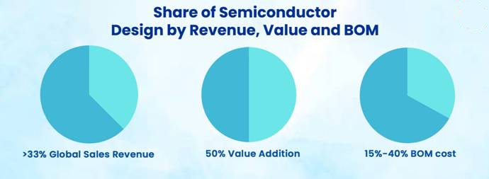
1. More than 50% of semiconductor value lies in design, architecture, and IP—not fabrication.
2. Fabless models require lower capital expenditure compared to fabs, but generate high value addition.
3. Control over design equals control over performance, security, energy efficiency, and system intelligence.
Without indigenous fabless capability, a country remains dependent on imported core technologies—even if chips are fabricated or assembled domestically. Hence, building a strong design ecosystem is essential for:
1. Technological sovereignty
2. IP ownership3
3. Import substitution
4. Attracting downstream manufacturing
5. Long-term innovation leadership

Design Linked Incentive (DLI) Scheme: Objectives and Architecture

The DLI Scheme, implemented by MeitY under the Semicon India Programme, aims to create a self-sustaining, innovation-driven semiconductor design ecosystem.
Core Objectives
1. Promote indigenous semiconductor design and IP creation.
2. Reduce India’s dependence on imported chips and IP cores.
3. Enable startups and MSMEs to move from concept to silicon.
4. Strengthen supply-chain resilience and domestic value addition.

Eligibility Framework

The scheme supports:
1. Startups (as per DPIIT norms).
2. MSMEs (as per MSME Ministry notification).
3. Domestic companies owned by resident Indian citizens.
4. t covers the entire design lifecycle, including:
Integrated Circuits (ICs)
1. Systems-on-Chip (SoCs)
2. Chipsets
3. Systems & semiconductor-linked designs
4. IP cores

Financial and Infrastructure Support under DLI

Component Sub-Category Key Provisions Purpose / Significance
Financial Support Product Design Linked Incentive (PDLI) • Reimbursement of up to 50% of eligible design expenditure
Cap: ₹15 crore per application
Reduces high upfront cost of chip design and encourages fabless startups
Deployment Linked Incentive (DLI) 4–6% incentive on net sales turnover
• Valid for 5 years
Cap: ₹30 crore per application
Promotes commercialization and market deployment of designed chips
Design Infrastructure Support ChipIN Centre (C-DAC) Central implementation agency for design infrastructure support Provides an end-to-end design ecosystem in India
National EDA Tool Grid Remote access to advanced Electronic Design Automation (EDA) tools Democratizes access to costly design software
IP Core Repository Reusable IP blocks for SoC development Speeds up design cycles and reduces duplication
MPW Prototyping Support Subsidized fabrication through global foundries Enables low-cost prototyping and testing
Post-Silicon Validation Testing, validation, and silicon bring-up support Improves reliability and readiness for commercial deployment

Programme Achievements and Ecosystem Impact

Infrastructure Democratization
1. 1 lakh+ engineers and students supported across 400 organizations.
2. World’s largest centralized chip-design user base.
3. 305 academic institutions under the Chips-to-Startup (C2S) programme.
4. 95 startups directly supported under DLI.
Innovation Outcomes
1. 10 patents filed
2. 16 chip tape-outs completed
3. 6 silicon-proven chips fabricated
4. 140+ reusable semiconductor IP cores developed
5. 1,000+ specialized engineers trained

Institutional Ecosystem Supporting Semiconductor Design

1. MeitY: Policy leadership and incentive frameworks.
2. Semicon India Programme (₹76,000 crore): End-to-end support for design, fabrication, and display manufacturing.
3. C-DAC: Nodal agency implementing DLI and ChipIN infrastructure.
4. Chips-to-Startup (C2S): Building 85,000 industry-ready chip-design professionals.
5. Microprocessor Development Programme: Indigenous RISC-V processors such as VEGA, SHAKTI, and AJIT.

Success Stories: From Indigenous Design to Global Relevance

1. Vervesemi: BLDC motor-control chips for consumer appliances and EVs.
2. InCore Semiconductors: Indigenous RISC-V processor IPs for edge-AI and smartphones.
3. Netrasemi: India’s first indigenously designed 12 nm AI surveillance SoC.
4. Aheesa Digital Innovations: Indigenous broadband SoCs for fiber connectivity.
5. AAGYAVISION: Radar-on-chip solutions for defence, drones, and smart infrastructure.

Strategic, Economic, and Geopolitical Dimensions

1. Strategic Autonomy: Reduced dependence on foreign IPs and chips. Assured access for defence, telecom, space, and AI.
2. Economic Impact: High-value job creation. Export-oriented deep-tech startups. Multiplier effect across electronics and manufacturing sectors.
3. Geopolitical Relevance: India positioned as a trusted semiconductor partner. Alignment with global supply-chain diversification strategies.

Challenges Ahead

1. Limited Domestic Fabrication Ecosystem: India’s semiconductor capabilities remain heavily skewed toward design, with advanced fabrication, packaging, and testing infrastructure still nascent. This forces fabless firms to rely on overseas foundries, increasing costs, lead times, and exposure to geopolitical risks.
2. Valley of Death between Design and Commercialization: Many startups face difficulties transitioning from successful tape-outs to market-ready products due to high costs of validation, certification, and system-level integration, limiting revenue realization.
3. Scaling from Pilot Production to Volume Manufacturing: Moving from MPW or pilot-lot fabrication to high-volume manufacturing requires assured demand, process maturity, yield optimization, and long-term foundry contracts—areas where early-stage firms struggle.
4. Access to Global Markets and Standards Compliance: Indian-designed chips often face challenges in meeting international certification, interoperability, and reliability standards, which are prerequisites for entry into global supply chains.
5. Sustained R&D Funding Constraints: Semiconductor R&D involves long gestation periods and high risk. Limited access to patient capital, especially for advanced-node and deep-tech designs, can slow innovation momentum.
6. Talent Retention and Brain Drain Risks: While India produces skilled design engineers, competition from global semiconductor firms and overseas opportunities poses challenges in retaining experienced talent within domestic startups.

Way Forward

1. Integrated Design–Fabrication–Packaging Ecosystem: Align DLI-supported designs with upcoming fabs, OSAT/ATMP units, and advanced packaging facilities in India to create an end-to-end domestic semiconductor value chain.
2. Market Pull through Government Procurement: Leverage defence, telecom, space, power, and digital public infrastructure procurement to create assured demand for indigenous chips, enabling startups to scale production.
3. Support for Advanced-Node and AI-Centric Designs: Expand DLI coverage and funding for advanced-node, AI/ML, automotive, and high-performance computing chips, ensuring relevance in future technology markets.
4. Global Market Access and Strategic Partnerships: Facilitate partnerships with global OEMs, system integrators, and standards bodies to help Indian firms meet certification requirements and integrate into international supply chains.
5. Long-Term R&D and Patient Capital Mechanisms: Create dedicated semiconductor innovation funds, blended finance models, and sovereign-backed venture capital to sustain long-term research and product development.
6. Deepened Industry–Academia–Defence Collaboration: Strengthen collaboration among startups, IITs, research labs, and defence institutions to accelerate innovation, talent development, and dual-use technology deployment.

Conclusion

The Design Linked Incentive (DLI) Scheme anchors India in the most strategic and value-intensive segment of the semiconductor value chain—chip design and intellectual property. By enabling startups and MSMEs to convert ideas into silicon-proven products, the scheme strengthens technological sovereignty, economic resilience, and global competitiveness. With tangible outcomes in patents, tape-outs, trained talent, and market-ready chips, DLI is transitioning India from a consumer of semiconductor technology to a creator of core digital intelligence. As India advances toward volume manufacturing and system-level integration, the DLI-driven ecosystem positions the country as a reliable, innovative, and strategic node in the global semiconductor landscape.

Prelims question:

Q. With reference to India’s Design Linked Incentive (DLI) Scheme for semiconductors, consider the following statements:
1. The scheme provides reimbursement of a portion of design expenditure incurred by fabless semiconductor companies.
2. It offers incentives linked to net sales turnover to encourage commercialization of indigenous chip designs.
3. The scheme is implemented by NITI Aayog under the National Policy on Electronics.
4. It supports access to Electronic Design Automation (EDA) tools and multi-project wafer (MPW) prototyping.
Which of the statements given above are correct?
A. 1, 2 and 4 only
B. 1 and 3 only
C. 2 and 3 only
D. 1, 2, 3 and 4

Answer: A

Mains Question:

Q. Fabless chip design lies at the core of semiconductor power and technological sovereignty.” In this context, examine the objectives, design architecture, and significance of India’s Design Linked Incentive (DLI) Scheme. Also discuss the key challenges in translating design capabilities into large-scale manufacturing and global competitiveness.

                                                                                                                                                                                                                                                                                                                                                                                                                                                        (250 words)

No Comments

Post A Comment