


12 Aug Indian Semiconductor Startups Raise $206M Since 2022: UPSC Current Affairs
✎ The Design-Linked Incentive (DLI) Scheme provides financial incentives to accelerate semiconductor design startups in India.
Subject Relevance — Where This Topic Fits
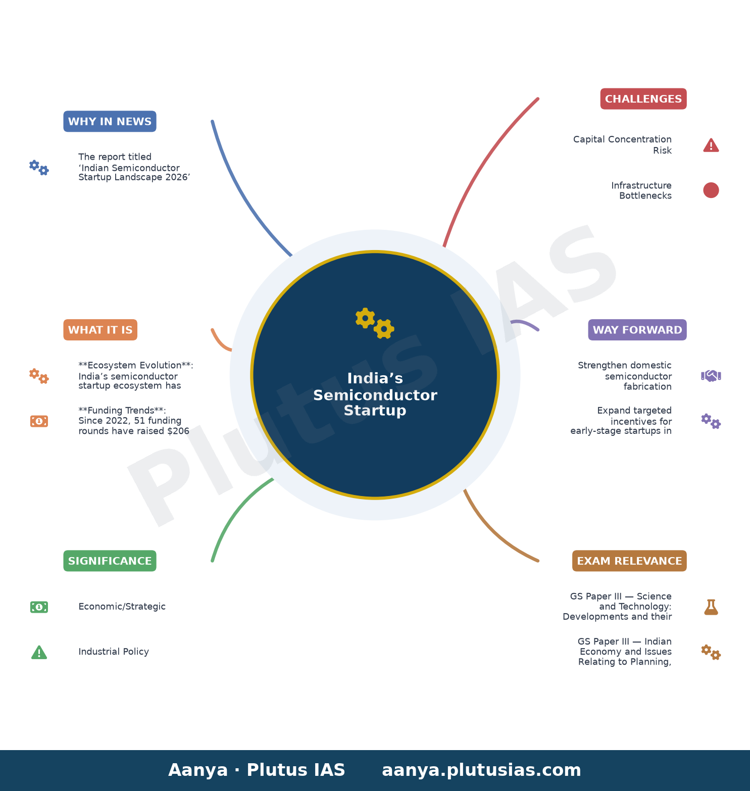
- GS Paper III — Science and Technology: Developments and their Applications and Effects in Everyday Life | GS Paper III — Indian Economy and Issues Relating to Planning, Mobilisation of Resources, Growth, Development and Employment | GS Paper III — Awareness in the fields of IT, Space, Computers, Robotics, Nano-technology, Bio-technology and Issues Relating to Intellectual Property Rights
- Prelims: Semiconductor manufacturing, Design-Linked Incentive (DLI) Scheme, RISC-V architecture, Fabrication (fab) units, Venture capital funding, Strategic disinvestment, Photonics in semiconductors, AI-driven chip design
- Essay: The Role of Government Incentives in Fostering Innovation and Entrepreneurship in India, Strategic Investments in Emerging Technologies: Balancing Public and Private Capital
Quick Revision: The Design-Linked Incentive (DLI) Scheme provides financial incentives to accelerate semiconductor design startups in India.
Why is this in the news?
The report titled ‘Indian Semiconductor Startup Landscape 2026’ by Speciale Invest and Startup Policy Forum highlights a significant surge in funding for homegrown semiconductor startups, with $206 million raised since 2022, including $61.9 million in the first half of 2026 alone. This trend underscores the maturing of India’s semiconductor ecosystem, driven by government-backed incentives, strategic investments, and a shift toward commercially viable ventures. The data reflects a strategic consolidation of capital in mature startups, particularly those supported by the Design-Linked Incentive (DLI) programme, and the emergence of new sub-sectors such as photonics and AI-driven chip design.
Background
- India’s semiconductor ecosystem has historically been dominated by design services, with limited manufacturing capacity; however, recent policy initiatives aim to expand both design and fabrication capabilities.
- The global semiconductor shortage during the COVID-19 pandemic highlighted the strategic importance of domestic semiconductor production, accelerating policy and investment responses worldwide.
- India’s semiconductor policy aligns with global trends such as the CHIPS Act in the United States and the European Chips Act, which aim to reduce dependence on foreign semiconductor supply chains.
Semiconductor Startups in India: Ecosystem, Incentives, and Strategic Investments
- **Ecosystem Evolution**: India’s semiconductor startup ecosystem has evolved from a services-centric model to one encompassing design, fabrication, and advanced applications. The first wave of startups focused on digital, RISC-V, and edge System-on-Chip (SoC) designs.
- **Funding Trends**: Since 2022, 51 funding rounds have raised $206 million, with $61.9 million raised in H1 2026 alone. The number of funding rounds has declined (16 in 2024, 13 in 2025, and 7 in H1 2026), but the average capital per round has increased, indicating a shift toward mature, commercially viable ventures.
- **Role of Government Incentives**: The Design-Linked Incentive (DLI) Scheme has been pivotal, with 24 chip-design projects supported under the programme. Of these, 14 have raised subsequent venture capital, totalling $100.8 million, demonstrating the scheme’s effectiveness in de-risking early-stage ventures and attracting private capital.
- **Strategic Investments**: Strategic investors, including global semiconductor firms and domestic technology companies (e.g., Zoho, TDK Ventures), are increasingly taking equity positions in Indian startups. These investments bring not only capital but also access to fabrication facilities (fabs), tool credits, reference customers, and design partnerships, enhancing the commercial viability of startups.
- **Sectoral Diversification**: The ecosystem is diversifying beyond traditional digital and RISC-V designs. This diversification aligns with global trends in semiconductor innovation.
- **Commercialisation and Scaling**: Several startups have demonstrated rapid scaling, moving from seed to Series A funding in 7 to 22 months. Seven recent Series A rounds totalled $73.7 million, representing one-third of all semiconductor startup capital raised since 2022, indicating growing investor confidence in commercially viable products.
- **Global Integration**: Indian semiconductor startups are increasingly integrating with global value chains. Global firms are establishing captive R&D centres in India and forming strategic partnerships with domestic startups, reflecting India’s growing role in the global semiconductor ecosystem.
Key Features
| Feature | Significance |
|---|---|
| Concentration of capital in mature ventures | Investors are prioritising later-stage semiconductor startups with proven product development and commercialisation potential, reducing dispersion of funds across early-stage ventures. |
| Government-linked incentives (DLI programme) | Design-Linked Incentive (DLI) support has catalysed private venture funding, with 14 of 24 DLI-backed chip-design projects securing institutional capital totalling $100.8 million. |
| Strategic investor participation | Global semiconductor firms and domestic corporations (e.g., Zoho, TDK Ventures) are taking equity stakes, providing access to fabrication facilities, tool credits, and design partnerships beyond financial capital. |
| Sectoral diversification | Emergence of startups in photonics, power semiconductors, fab tooling, metrology, AI data-centre silicon, and analogue AI inference, expanding beyond traditional digital and RISC-V domains. |
| Accelerated funding cycles | Multiple startups have transitioned from seed to Series A funding within 7–22 months, indicating rapid maturation of the ecosystem. |
Why it Matters
Economic/Strategic
- Demonstrates India’s evolving capacity to develop indigenous semiconductor capabilities, reducing import dependence in critical technology sectors.
- Attracts global strategic investors, positioning India as a viable alternative to established semiconductor hubs for design and R&D.
- Supports the government’s vision of a self-reliant (Atmanirbhar Bharat) semiconductor ecosystem through public-private partnerships.
Industrial Policy
- Validates the efficacy of targeted incentives like the Design-Linked Incentive (DLI) scheme in bridging the funding gap for high-risk, capital-intensive ventures.
- Highlights the role of incubation and policy frameworks in nurturing deep-tech startups beyond generic startup ecosystems.
Investment Ecosystem
- Signals maturation of India’s venture capital landscape, with investors adopting sector-specific concentration strategies rather than broad diversification.
- Encourages follow-on investments in high-potential startups, fostering a virtuous cycle of capital deployment and innovation.
Technological Sovereignty
- Advances India’s position in critical semiconductor value chains, particularly in design, AI-driven silicon, and specialised hardware.
- Reduces reliance on foreign semiconductor imports for strategic sectors such as defence, telecommunications, and data infrastructure.
Challenges
1. Capital Concentration Risk
- Over-reliance on a small cohort of mature startups (e.g., C2i Semiconductors, NetraSemi) may create systemic fragility if these ventures underperform.
- Early-stage startups in novel domains (e.g., photonics, metrology) may face prolonged funding gaps, stifling innovation in emerging segments.
UPSC Link: GS3: Startup ecosystem challenges
2. Infrastructure Bottlenecks
- Limited domestic fabrication capacity (fabs) restricts the ability of Indian startups to scale production locally, necessitating partnerships with foreign fabs.
- Dependence on imported semiconductor tools and materials increases vulnerability to global supply chain disruptions.
UPSC Link: GS3: Manufacturing infrastructure gaps
3. Talent and R&D Deficit
- Shortage of specialised talent in semiconductor design, AI-led silicon, and fab operations constrains growth despite funding availability.
- Inadequate collaboration between academia (e.g., IITs, IISc) and industry limits the translation of research into commercial products.
UPSC Link: GS3: Skill gaps in STEM sectors
4. Regulatory and Policy Hurdles
- Complexity in availing incentives under schemes like DLI may deter smaller startups from participating due to compliance burdens.
- Uncertainty in intellectual property (IP) frameworks for semiconductor designs could discourage strategic investors from long-term commitments.
UPSC Link: GS2: Regulatory ease for startups
5. Global Competition
- Aggressive incentives from countries like the US (CHIPS Act), China, and South Korea pose a risk of talent and capital flight from India.
- Geopolitical tensions may restrict access to critical semiconductor materials and equipment from dominant global suppliers.
UPSC Link: GS2: Foreign policy and tech sovereignty
Challenges — UPSC Perspective
| Issue | Concern |
|---|---|
| Limited fab capacity | Restricts local production scaling; startups must rely on foreign fabrication partners. |
| Talent scarcity in niche domains | Delays product development and commercialisation in emerging sectors like photonics and AI silicon. |
| High capital intensity | Deters early-stage startups from pursuing capital-intensive R&D in semiconductor design. |
| Intellectual property risks | Uncertainty in IP protection may deter strategic investors from equity participation. |
| Supply chain vulnerabilities | Dependence on imported tools and materials exposes startups to global price volatility. |
| Policy compliance complexity | Bureaucratic hurdles in availing government incentives may exclude smaller players. |
Way Forward
- Strengthen domestic semiconductor fabrication infrastructure through public-private partnerships to reduce reliance on foreign fabs.
- Expand targeted incentives for early-stage startups in emerging domains (e.g., photonics, metrology) to diversify the ecosystem.
- Enhance collaboration between academic institutions (IITs, IISc) and industry to bridge the talent and R&D deficit.
- Simplify compliance frameworks for government schemes like DLI to ensure broader participation, especially for smaller startups.
- Develop a national semiconductor talent development programme in partnership with global semiconductor firms to address skill gaps.
- Establish a dedicated semiconductor innovation fund to provide seed-stage capital for high-risk, high-reward ventures.
- Negotiate long-term supply agreements for critical semiconductor materials and equipment to mitigate import dependency.
- Promote international collaborations to access advanced fabrication technologies and joint R&D initiatives.
UPSC Value Addition
Keywords for Mains Answer-Writing
Semiconductor industry in India · Design-Linked Incentive (DLI) Scheme · Startup ecosystem in electronics manufacturing · Venture capital in semiconductor startups · Atmanirbhar Bharat in electronics · Semiconductor fabs and design · Government incentives for semiconductor ecosystem · Strategic investments in startups · RISC-V architecture in India · Photonics and compound semiconductors in India
Concept Flow
Government announces semiconductor incentives (e.g., DLI scheme) → Early-stage startups emerge in design and niche domains → Investors assess maturity and commercial potential → Capital concentrates in proven ventures → Strategic investors (global and domestic) take equity stakes → Ecosystem diversifies into photonics, AI silicon, etc. → Accelerated funding cycles validate sector maturity → Policy frameworks adapt to emerging challenges
Prelims Practice Questions
Q1. Consider the following statements regarding the Design-Linked Incentive (DLI) Scheme in India:
1. The DLI Scheme provides financial incentives to semiconductor startups for product design and development.
2. The scheme is administered by the Ministry of Electronics and Information Technology (MeitY).
3. As of 2026, 24 chip-design projects have been supported under the DLI Scheme.
4. The DLI Scheme exclusively funds early-stage startups and does not support mature ventures.
How many of the above statements are correct?
- Only one
- Only two
- Only three
- All four
Answer: Only three — Statements 1, 2, and 3 are correct. Statement 4 is incorrect as the DLI Scheme supports both early-stage and mature ventures, with a focus on product development and commercialization.
Q2. Assertion (A): The Indian semiconductor startup ecosystem has witnessed a decline in the number of funding rounds since 2024, despite an increase in capital deployed.
Reason (R): Investors are increasingly concentrating capital in mature semiconductor ventures with proven product development and commercialization, rather than spreading bets across early-stage startups.
In the context of the above two statements, which one of the following is correct?
- Both A and R are true, and R is the correct explanation of A
- Both A and R are true, but R is not the correct explanation of A
- A is true, but R is false
- A is false, but R is true
Answer: Both A and R are true, and R is the correct explanation of A — Both the Assertion (A) and Reason (R) are true, and the Reason (R) correctly explains the Assertion (A). The decline in the number of funding rounds is attributed to investors’ preference for mature ventures with proven commercial viability.
Q3. Match the following semiconductor-related initiatives in India with their respective ministries/departments:
Column I (Initiative) Column II (Ministry/Department)
A. Semicon India Programme 1. Ministry of Science and Technology
B. Design-Linked Incentive (DLI) Scheme 2. Ministry of Electronics and Information Technology (MeitY)
C. National Mission on Interdisciplinary Cyber-Physical Systems (NM-ICPS) 3. Ministry of Education
D. Atal Innovation Mission (AIM) 4. NITI Aayog
- A-2, B-2, C-1, D-4; A-2, B-2, C-4, D-1; A-1, B-2, C-4, D-3; A-2, B-1, C-4, D-3
- answer_string_array_indexed_by_q_indexes_above
- explain_match_pairs_in_skeleton
- format_match
Answer: ? — A. Semicon India Programme is administered by the Ministry of Electronics and Information Technology (MeitY).
B. Design-Linked Incentive (DLI) Scheme is also administered by MeitY.
C. National Mission on Interdisciplinary Cyber-Physical Systems (NM-ICPS) falls under the Ministry of Science and Technology.
D. Atal Innovation Mission (AIM) is a flagship initiative of NITI Aayog.
Mains Practice Question
✍ The Indian semiconductor startup ecosystem has demonstrated a paradoxical trend: a decline in the number of funding rounds alongside a significant increase in capital deployment since 2022. Critically analyse the factors driving this trend and examine its implications for India’s ambition to become a global hub for semiconductor design and manufacturing. (15 Marks)
Approach: MODEL-ANSWER SKELETON:
1. **Introduction (2 Marks)**
– Briefly define the semiconductor startup ecosystem in India and its strategic importance under Atmanirbhar Bharat.
– Present the paradox: fewer rounds, higher capital (data from the report: 51 rounds, $206 million since 2022; H1 2026 alone raised $61.9 million, 81% of 2025 total).
2. **Drivers of the Trend (6 Marks)**
– **Investor Preference for Mature Ventures**: Investors are concentrating capital in companies with advanced product development and commercialization (e.g., C2i Semiconductors, NetraSemi, Morphing Machines, Mindgrove Technologies).
– **Government Support Mechanisms**: Role of the Design-Linked Incentive (DLI) Scheme—24 chip-design projects supported, 14 raised $100.8 million; 6 closed follow-on rounds worth $53.6 million. Strategic investors (e.g., Zoho, TDK Ventures) and global semiconductor firms are increasingly taking equity positions.
– **Sectoral Maturity**: Emergence of new domains (photonics, power semiconductors, AI data-centre silicon) and acceleration from seed to Series A (7–22 months).
– **Strategic Capital Benefits**: Access to fabs, tool credits, reference customers, and design partnerships.
3. **Implications for India’s Semiconductor Ambition (5 Marks)**
– **Positive Implications**:
– Focus on high-potential ventures reduces risk of capital dispersion and increases likelihood of success.
– Strengthens India’s position in global semiconductor value chains (e.g., AI-led design workflows, RISC-V architecture).
– Alignment with government’s Semicon India Programme and PLI schemes.
– **Challenges and Risks**:
– Early-stage startups may face funding gaps, limiting innovation diversity.
– Over-reliance on government incentives could create dependency.
– Need for sustained investment in R&D infrastructure and talent development.
4. **Conclusion (2 Marks)**
– The trend reflects a maturing ecosystem but requires balanced policy and investment to ensure inclusivity and long-term sustainability. Highlight the need for continued support to early-stage ventures while leveraging the momentum in mature segments.
Source: Business Standard
Generated by AanyaAi for educational purpose.

- Gurugram’s groundwater extraction exceeds limit by 212%; HC seeks ban - October 4, 2026
- स्वतंत्रता सेनानी श्यामजी कृष्ण वर्मा की जन्म जयंती पर पीएम का श्रद्धांजलि - October 4, 2026
- KWML’s Feasibility Reports for Water Metro in 18 Cities: UPSC & PCS Insights - October 3, 2026
No Comments