


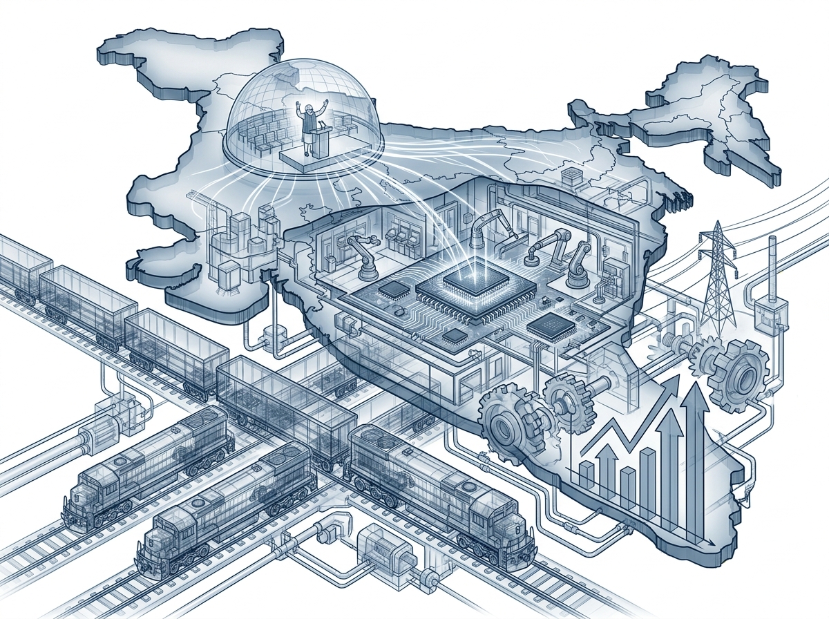
17 Sep PM Modi highlights India’s 7.8% growth & semiconductor push at SEMICON India 2026
✎ India’s Semiconductor Mission (Semicon 2.0) targets 200 chip-design startups, and 85,000 trained engineers, aiming to integrate India into the global semiconductor value chain while enhancing economic resilience.
Subject Relevance — Where This Topic Fits
- GS Paper II — International Relations (BRICS, global economic confidence) | GS Paper III — Indian Economy (growth, manufacturing, logistics, startups, sovereign ratings)
- Prelims: Semiconductor Mission India, Dedicated Freight Corridors (DFC), New Delhi Declaration, sovereign credit rating, electronic design automation (EDA), fab, packaging, chip design, venture capital funding
- Essay: Technological self-reliance and India’s role in the global semiconductor value chain, Infrastructure-led growth: freight corridors, logistics, and manufacturing competitiveness
Quick Revision: India’s Semiconductor Mission (Semicon 2.0) targets 200 chip-design startups, and 85,000 trained engineers, aiming to integrate India into the global semiconductor value chain while enhancing economic resilience.
Why is this in the news?
The inauguration of SEMICON India 2026 by the Prime Minister, coupled with the announcement of Semicon 2.0 and the release of India’s latest quarterly GDP growth figure of 7.8%, underscores the intersection of industrial policy, technological advancement, and macroeconomic performance. The event highlights India’s strategic push to integrate into the global semiconductor supply chain, while also reflecting broader economic reforms aimed at enhancing logistics infrastructure, fintech innovation, and manufacturing competitiveness.
Background
- India’s GDP growth of 7.8% in the latest quarter, reported by the National Statistical Office (NSO), reflects resilience amid global economic headwinds, including geopolitical tensions and supply chain disruptions.
- The operationalisation of approximately 3,000 km of Dedicated Freight Corridors (DFCs) under the Dedicated Freight Corridor Corporation of India (DFCCIL) aims to decongest rail networks, reduce logistics costs, and accelerate freight movement across key industrial hubs.
- The Global FinTech Fest in Mumbai focused on inclusive finance, agentic AI, tokenisation, and quantum technology, signalling India’s ambition to become a global fintech hub.
- The New Delhi Declaration adopted at the BRICS Summit reaffirmed commitments to multilateralism, sustainable development, and technological cooperation, enhancing India’s diplomatic and economic standing.
- Sovereign credit rating upgrades by international agencies (e.g., Moody’s, S&P, or Fitch) in 2025-26 reflect improved investor confidence in India’s macroeconomic stability and policy direction.
What is Semicon 2.0 and India’s Semiconductor Ecosystem?
- Semicon 2.0 is the second phase of India’s Semiconductor Mission, launched to consolidate and expand the domestic semiconductor ecosystem across six verticals: chip design, manufacturing equipment and materials, fabrication (fabs), advanced packaging, research and development (R&D), and talent development.
- The programme aims to support at least 200 chip-design startups and companies, with 70,000 engineers having been trained in four years against an initial target of 85,000 design engineers over a 10-year period.
- Over 400 universities across India now have access to Electronic Design Automation (EDA) tools, enabling academic institutions to participate in semiconductor design and innovation.
- The first phase of the Semiconductor Mission engaged more than 105 startups, with around 20 securing venture capital funding totalling approximately ₹800 crore, indicating growing investor interest in the sector.
- India’s semiconductor strategy is aligned with global supply chain diversification efforts, reducing dependence on geopolitically sensitive regions and enhancing self-reliance in critical technologies.
- The Semiconductor Mission is implemented by the Ministry of Electronics and Information Technology (MeitY) in collaboration with state governments, industry associations (e.g., India Electronics and Semiconductor Association), and international partners.
Key Features
| Feature | Significance |
|---|---|
| 7.8% GDP growth in latest quarter | Demonstrates macroeconomic resilience amid global headwinds, reinforcing India’s position as a high-growth major economy. |
| Semiconductor ecosystem development (Semicon 2.0) | Aims to establish India as a global semiconductor hub by fostering chip design, fabs, packaging, and R&D capabilities. |
| 3,000 km dedicated freight corridors | Enhances logistics efficiency, reduces transit time, and lowers logistics costs, directly supporting manufacturing and trade competitiveness. |
| Global FinTech Fest 2026 (Mumbai) | Showcases India’s leadership in inclusive financial technologies, including AI-driven agentic models, tokenisation, and quantum computing applications. |
| Sovereign rating upgrade by credit agency | Reflects improved investor confidence in India’s economic fundamentals and long-term growth prospects. |
Why it Matters
Economic Resilience and Growth
- The 7.8% growth rate underscores India’s ability to sustain high growth despite global economic volatility, supply chain disruptions, and geopolitical tensions.
- A sovereign rating upgrade signals reduced perceived risk, potentially lowering borrowing costs for government and private sector entities.
- Operationalisation of freight corridors and logistics improvements directly enhance ease of doing business, attracting investment in manufacturing and exports.
Strategic Industrialisation
- The semiconductor push aligns with India’s vision to reduce import dependence in critical technologies, particularly in electronics and defence manufacturing.
- Semicon 2.0’s six-pillar approach (design, fabs, materials, packaging, R&D, talent) ensures a comprehensive ecosystem, not just assembly or packaging.
- Training 70,000 design engineers in four years (against a 10-year target) demonstrates accelerated capability-building in high-tech domains.
Global Positioning and Diplomacy
- Hosting the BRICS Summit and adoption of the New Delhi Declaration by consensus highlights India’s growing diplomatic influence and multilateral engagement.
- Participation of 105 startups in the semiconductor programme, with 20 securing venture capital funding, signals international investor interest in India’s tech ecosystem.
- The phrase ‘India’s chips will go out to the world’ encapsulates the export-oriented industrialisation strategy for high-value manufacturing.
Technological and Financial Innovation
- Focus on agentic AI, tokenisation, and quantum technology in fintech underscores India’s transition toward a digital-first financial architecture.
- Access to electronic design automation (EDA) tools in 400+ universities democratises semiconductor design education, fostering grassroots innovation.
- Venture capital infusion of ₹800 crore into semiconductor startups indicates a maturing innovation ecosystem with commercial viability.
Challenges
1. Semiconductor Manufacturing Scale-Up
- High capital intensity and long gestation periods for semiconductor fabrication plants (fabs) pose financial and risk management challenges.
- Dependence on imported semiconductor manufacturing equipment and raw materials (e.g., silicon wafers) creates supply chain vulnerabilities.
- Competition from established global players (e.g., TSMC, Intel) requires India to offer competitive incentives and policy stability to attract investments.
UPSC Link: GS3: Industrial Policy, Manufacturing
2. Logistics and Infrastructure Bottlenecks
- Despite freight corridor operationalisation, last-mile connectivity, multi-modal integration, and port efficiency remain critical gaps.
- High logistics costs (estimated at 13-14% of GDP) continue to erode competitiveness, particularly for MSMEs and export-oriented industries.
- Digital integration across logistics stakeholders (e.g., customs, transporters, warehouses) requires sustained policy and technological coordination.
UPSC Link: GS3: Infrastructure, Logistics
3. Talent and Skill Development Gaps
- While 70,000 engineers have been trained, the demand for advanced semiconductor design and fabrication skills far exceeds supply.
- Retention of skilled professionals in high-tech sectors is challenged by competition from global firms and higher compensation abroad.
- Curriculum alignment with industry needs in universities requires continuous updating, particularly in emerging domains like quantum computing.
UPSC Link: GS2: Education, Skill Development
4. Geopolitical and Trade Risks
- US-China tensions and export controls (e.g., on advanced semiconductor equipment) may disrupt global supply chains critical to India’s ambitions.
- Over-reliance on a single market (e.g., China) for raw materials or intermediate goods could expose India to trade disruptions.
- Balancing strategic autonomy with global integration in semiconductor supply chains requires careful policy navigation.
UPSC Link: GS2: International Relations, GS3: Security
5. Financial and Fiscal Sustainability
- Large-scale public investment in semiconductor fabs and infrastructure demands efficient capital allocation and risk-sharing mechanisms.
- Ensuring viability of startups in capital-intensive sectors like semiconductors requires a balanced approach between subsidies and market-driven growth.
- Sovereign rating upgrades are contingent on sustained fiscal discipline and inflation control, which remain policy priorities.
UPSC Link: GS3: Economic Reforms, Fiscal Policy
Challenges — UPSC Perspective
| Issue | Concern |
|---|---|
| Capital intensity of semiconductor fabs | High upfront investment and long payback periods deter private sector participation. |
| Supply chain dependencies | Import reliance on critical inputs (e.g., semiconductor equipment, rare earths) creates geopolitical exposure. |
| Logistics cost and efficiency | High costs and inefficiencies in freight movement undermine manufacturing competitiveness. |
| Skill shortages in high-tech domains | Gap between industry demand and educational output limits ecosystem growth. |
| Geopolitical trade constraints | Export controls and sanctions (e.g., US-China) may disrupt global semiconductor supply chains. |
| Policy stability and incentives | Consistency in PLI schemes, tax regimes, and ease of doing business is critical for investor confidence. |
Government Initiatives — Must-Memorise for Prelims
- Semiconductor Mission (Semicon 2.0)
- Production-Linked Incentive (PLI) Scheme for Electronics and Semiconductors
- Dedicated Freight Corridor Project
- National Logistics Policy
Way Forward
- Accelerate the operationalisation of semiconductor fabs by streamlining regulatory approvals (e.g., land acquisition, environmental clearances) and offering viability gap funding.
- Expand the PLI scheme to include ancillary industries (e.g., semiconductor equipment manufacturing, advanced packaging materials) to create a self-sustaining ecosystem.
- Strengthen multi-modal logistics infrastructure by integrating freight corridors with ports, airports, and industrial corridors to reduce transit times and costs.
- Scale up skill development initiatives through public-private partnerships, focusing on semiconductor design, fabrication, and advanced packaging technologies.
- Enhance global supply chain resilience by diversifying sourcing of critical inputs (e.g., silicon wafers, rare earths) and negotiating long-term trade agreements.
- Promote R&D collaboration between industry and academia (e.g., IITs, IISc) to develop indigenous semiconductor technologies and reduce import dependence.
- Establish a dedicated semiconductor export promotion council to identify target markets, negotiate trade agreements, and facilitate market access for Indian chips.
UPSC Value Addition
Keywords for Mains Answer-Writing
Semiconductor Mission India · Semicon 2.0 Policy Framework · Chip Design Ecosystem · Electronic Design Automation (EDA) Tools · Dedicated Freight Corridors (DFC) · Global Semiconductor Supply Chain · Venture Capital in Semiconductor Startups · Sovereign Credit Rating Upgrade · New Delhi Declaration of BRICS · Electronics Manufacturing Clusters (EMC) · National Policy on Electronics 2019 · Production-Linked Incentive (PLI) Scheme for Semiconductors
Concept Flow
Global economic volatility and geopolitical tensions → India’s high GDP growth (7.8%) → Demonstrates macroeconomic resilience and investor confidence. → Investor confidence → Sovereign rating upgrade → Lower borrowing costs and improved access to capital for domestic industries. → Government’s strategic push for semiconductor self-reliance → Semicon 2.0 initiative → Six-pillar ecosystem development (design, fabs, materials, packaging, R&D, talent). → Semiconductor ecosystem growth → Training 70,000 engineers, 400+ universities with EDA tools → Addresses skill shortages and fosters innovation. → Operationalisation of 3,000 km freight corridors → Reduced logistics costs and transit times → Enhances manufacturing competitiveness and export potential. → BRICS Summit and New Delhi Declaration → Multilateral engagement and global positioning → Reinforces India’s role in shaping global supply chain narratives. → Fintech innovation (agentic AI, tokenisation, quantum tech) → Digital financial inclusion → Supports broader economic formalisation and growth.
Prelims Practice Questions
Q1. Consider the following statements regarding India’s Semiconductor Mission:
1. The Semicon 2.0 policy framework aims to support at least 200 chip-design startups and companies.
2. Over 400 universities in India now have access to Electronic Design Automation (EDA) tools.
3. The mission targets training 85,000 design engineers in a span of 10 years.
How many of the above statements are correct?
- Only one
- Only two
- All three
- None
Answer: All three — Statement 1 and 2 are correct as per the Semicon 2.0 framework. Statement 3 is incorrect because the target of 85,000 design engineers was initially set for a 10-year period, but India has already trained 70,000 engineers in four years, indicating an accelerated pace.
Q2. Assertion (A): The operationalisation of Dedicated Freight Corridors (DFC) in India is expected to significantly improve logistics efficiency.
Reason (R): DFCs are designed to provide faster and more reliable freight movement by segregating freight and passenger traffic.
- Both A and R are true, and R is the correct explanation of A
- Both A and R are true, but R is not the correct explanation of A
- A is true, but R is false
- A is false, but R is true
Answer: Both A and R are true, and R is the correct explanation of A — Both the assertion and reason are correct. The operationalisation of DFCs is indeed expected to improve logistics efficiency by segregating freight and passenger traffic, leading to faster and more reliable freight movement.
Q3. Which of the following is NOT one of the six pillars of India’s Semiconductor Mission under Semicon 2.0?
A. Chip design
B. Advanced packaging
C. Quantum computing hardware
D. Research and development
- A
- B
- C
- D
Answer: C — Quantum computing hardware is not listed as one of the six pillars of India’s Semiconductor Mission under Semicon 2.0. The pillars are chip design, machines and materials, fabs, advanced packaging, research and development, and talent.
Mains Practice Question
✍ Critically examine the role of the Semiconductor Mission India in transforming the country into a global hub for semiconductor design and manufacturing. Also, assess the challenges that may impede its success. (15 Marks)
Approach: MODEL-ANSWER SKELETON:
1. **Introduction**: Define the Semiconductor Mission India and its objectives under Semicon 2.0, including the six pillars (chip design, machines and materials, fabs, advanced packaging, R&D, and talent).
2. **Transformative Role**:
– **Chip Design Ecosystem**: Highlight the growth in chip-design startups (e.g., over 105 startups in Phase 1, 20 securing VC funding of ~Rs 800 crore) and the training of 70,000 design engineers in four years.
– **Infrastructure**: Mention the access to Electronic Design Automation (EDA) tools in over 400 universities and the operationalisation of Dedicated Freight Corridors (DFC) to improve logistics.
– **Global Confidence**: Discuss the sovereign credit rating upgrade and India’s role in the New Delhi Declaration of BRICS as indicators of growing international trust.
3. **Challenges**:
– **Infrastructure Gaps**: Highlight the need for advanced manufacturing facilities (fabs) and the dependence on imported machinery and materials.
– **Talent Shortage**: Despite progress, the demand for skilled engineers and researchers remains high.
– **Global Competition**: Competition from established semiconductor hubs like Taiwan, South Korea, and the US.
– **Policy Implementation**: Challenges in translating policy frameworks into tangible outcomes, including regulatory hurdles and bureaucratic delays.
4. **Conclusion**: Summarise the mission’s potential to position India as a global semiconductor hub while acknowledging the need for sustained efforts to overcome structural challenges.
Source: orissapost.com
Generated by AanyaAi for educational purpose.
Related guides on our sites
- Best economics services coaching
- Best economics optional coaching
- Best economics optional coaching for upsc
- best teacher of economics optional

- PM Modi highlights India’s 7.8% growth & semiconductor push at SEMICON India 2026 - September 17, 2026
- गृहमंत्रालय ने ठुकराया दारा सिंह का रिहाई निवेदन, जानिए पूरा मामला - September 17, 2026
- Odisha Rejects Dara Singh’s Remission Plea in Graham Staines Case: SC Hearing - September 17, 2026
No Comments