Background: Quantum Light and Photonics
1. Quantum Light Defined: Quantum light consists of individual photons exhibiting non-classical properties like entanglement and superposition, essential for encoding and processing quantum information.
2. Correlated Photon Pairs: Photon pairs, often generated via spontaneous four-wave mixing, are entangled or time-correlated and serve as fundamental resources in quantum computing, quantum communication, and quantum sensing.
3. Quantum Communication Use: Correlated photons enable ultra-secure communication protocols like quantum key distribution (QKD), as any attempt at interception disturbs the quantum state and can be detected.
4. Quantum Sensing Applications: Entangled photons enhance sensitivity and precision in measurements, making them valuable in quantum-enhanced sensing technologies such as interferometry and biomedical imaging.
5. Role of Photonics: Photonic circuits guide and manipulate light on-chip using tiny optical structures, enabling compact, high-speed, and energy-efficient quantum systems without bulky external optics.
6. Microring Resonators: These tiny optical loops confine light and enhance nonlinear interactions, efficiently generating photon pairs in a compact area, making them ideal for on-chip quantum light sources.
7. Temperature Sensitivity: Microring resonators are highly sensitive to temperature changes; even slight fluctuations can detune their resonance, disrupting photon-pair generation.
8. Fabrication Challenges: Variations in chip manufacturing processes can cause inconsistencies in photonic device performance, requiring external stabilization and limiting scalability in traditional quantum setups.
The Breakthrough: A Quantum Light Factory on Chip
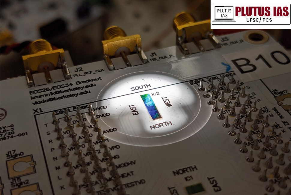
1. Compact Integration: The chip integrates quantum light sources (microring resonators), photodiodes, and classical electronic control circuits into a tiny 1×1 mm² silicon area, enabling complete quantum light generation and control on a single platform.
2. Microring Resonators as Photon Factories: Each of the 12 microring resonators on the chip serves as a “quantum light factory”, generating streams of correlated photon pairs required for quantum applications.
3. On-Chip Photodiodes for Monitoring: Photodiodes are embedded directly inside the microrings to monitor alignment with the incoming laser light in real time, ensuring precise resonance tuning.
4. Real-Time Feedback Control: The chip features on-chip heaters and control logic that actively adjust each resonator’s frequency to correct for temperature drift and fabrication-induced variations.
5. Parallel Quantum Light Generation: All 12 photon-pair sources on the chip can operate in parallel, without interfering with each other, enabling scalable and synchronized quantum operations.
6. Standard CMOS Process: Fabricated using a 45-nanometer commercial CMOS process, the chip demonstrates that advanced quantum photonic systems can be built using conventional semiconductor foundries, paving the way for mass production.
7. Scalability and Stability: This integration ensures that the quantum system is robust, repeatable, and temperature-resilient, addressing key barriers to building larger and more complex chip-based quantum architectures.
Technical Features and Design Innovations
1. Photodiode-Driven Resonance Monitoring: Each microring resonator contains an embedded photodiode that detects deviations in alignment with the incoming laser, allowing real-time monitoring of optical resonance conditions.
2. On-Chip Thermal Tuning: Micro-heaters are integrated alongside the resonators to dynamically adjust their temperature, thereby correcting any frequency drift and maintaining consistent quantum light generation.
3. Real-Time Feedback Loop: The chip features a closed-loop control system combining photodiode input with on-chip electronics to ensure continuous tuning and stabilization during operation.
4. Unified CMOS-Compatible Design: The entire system, including quantum photonics and control electronics, was co-designed to fit within the strict layout rules of the 45-nanometer CMOS process, ensuring manufacturability at scale.
5. Parallel Source Operation: All 12 quantum light sources are independently stabilized and can function simultaneously, enhancing the chip’s capacity for multi-channel quantum information processing.
6. Minimized Crosstalk and Interference: The design addresses challenges like thermal crosstalk between nearby resonators, ensuring stable operation across the chip even in a compact footprint.
7. Link with AI-Optical Interconnects: Developed in part with Ayar Labs, the same chip platform that supports AI optical interconnects now demonstrates the feasibility of building quantum photonic systems, bridging AI and quantum hardware.
Significance and Potential Applications
1. Scalable Quantum Hardware: This chip demonstrates that quantum photonic systems can be stabilized and mass-produced using commercial CMOS foundries, a key step toward scalable quantum devices.
2. Quantum Computing Infrastructure: The integrated chip serves as a core component in building future quantum processors, where stable photon sources are essential for implementing qubits and logic gates.
3. Quantum-Secure Communications: It enables secure communication protocols like Quantum Key Distribution (QKD), which rely on entangled photon pairs to detect eavesdropping and ensure data privacy.
4. Precision Sensing and Metrology: The chip can be used in quantum-enhanced sensors for applications such as biological imaging, gravimetry, and time synchronization, offering superior accuracy and sensitivity.
5. AI and HPC Optical Interconnects: The same silicon photonics infrastructure that powers this chip can be used for high-speed optical data transmission in AI and supercomputing systems, boosting performance while reducing power consumption.
6. Modular Quantum Networks: The chip’s ability to operate multiple quantum sources in parallel makes it ideal for building modular, multi-chip quantum systems, a critical need for networked quantum computing.
7. Research and Industrial Impact: This success bridges the gap between lab-scale quantum research and commercial-grade chip manufacturing, accelerating the transition to practical quantum technologies for academia and industry alike.
The Power of Interdisciplinary Collaboration
1. Cross-Domain Integration: The project brought together expertise from quantum optics, photonics, and electronic engineering, disciplines that typically operate in silos.
2. Academic Synergy: Researchers from Boston University, UC Berkeley, and Northwestern University contributed complementary strengths in chip design, quantum measurement, and photonic integration.
3. Industry Collaboration: Close partnerships with GlobalFoundries (CMOS fabrication), Ayar Labs (optical chiplets), and PsiQuantum (quantum computing) enabled real-world deployment of cutting-edge research.
4. Unified System Design: The success relied on the co-design of electronics and photonics, tailored to operate seamlessly within a standard CMOS platform.
5. Scalable Manufacturing: Collaboration with semiconductor foundries ensured the quantum chip could be fabricated using mass-producible commercial processes.
6. Quotable Insights: Miloš Popović noted the significance of building quantum systems in standard foundries; Anirudh Ramesh emphasized real-time, on-chip control; Prem Kumar praised the deep interdisciplinary cooperation.
7. Model for Future Innovation: The project sets a precedent for interdisciplinary research models, necessary for transitioning quantum technology from lab-scale to scalable industrial applications.
Industry Impact and Future Trajectories
1. Student Career Outcomes: Graduates from the project have joined top companies: PsiQuantum, Ayar Labs, Aurora, and Google X, contributing to quantum computing and photonics innovation.
2. Industrial Skill Pipeline: The project nurtured highly skilled engineers now applying their knowledge in cutting-edge quantum and optical hardware companies, bridging academia and industry.
3. Silicon Photonics Momentum: There’s rising demand for silicon photonics as a scalable platform for both quantum light generation and AI optical interconnects.
4. Multi-Chip Quantum Systems: The ability to operate multiple sources in parallel hints at future architectures where interconnected quantum chips perform coordinated tasks.
5. Quantum Networking Potential: With stable, on-chip photon sources, the foundation is laid for chip-scale quantum communication networks and quantum internet prototypes.
6. Convergence with AI: The overlap between photonics for quantum and AI compute acceleration signals a converging future where these technologies enhance one another.
7. Driving Scalable Quantum Infrastructure: The chip’s demonstration of stability, repeatability, and integration within CMOS sets the stage for industrial-scale quantum infrastructure development.
Conclusion
The integration of quantum light sources with classical electronics on a CMOS chip marks a key step toward scalable quantum technology. Developed by researchers at Northwestern, BU, and UC Berkeley, the chip is compact, stable, and manufacturable using standard processes. It overcomes major technical hurdles and enables practical applications in quantum computing, secure communication, sensing, and AI. This innovation lays the foundation for future modular quantum systems and highlights the power of interdisciplinary collaboration in advancing next-gen quantum technologies.
Prelims Questions


No Comments