
19 Jul Towards Scalable Quantum Technologies: Integrating Quantum Light Sources and Control Electronics on a Silicon Chip
This article covers “Daily Current Affairs” and the topic Towards Scalable Quantum Technologies: Integrating Quantum Light Sources and Control Electronics on a Silicon Chip
SYLLABUS MAPPING:
GS-3- Science and technology- Towards Scalable Quantum Technologies: Integrating Quantum Light Sources and Control Electronics on a Silicon Chip
FOR PRELIMS
What is special about the new chip that can make and control quantum light?
FOR MAINS
What are the challenges in making quantum chips, and how does this chip deal with them?
Why in the News?
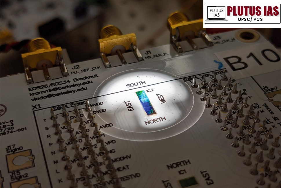
The Breakthrough: A Quantum Light Factory on Chip
Technical Features and Design Innovations
1. Photodiode-Driven Resonance Monitoring: Each microring resonator contains an embedded photodiode that detects deviations in alignment with the incoming laser, allowing real-time monitoring of optical resonance conditions.
2. On-Chip Thermal Tuning: Micro-heaters are integrated alongside the resonators to dynamically adjust their temperature, thereby correcting any frequency drift and maintaining consistent quantum light generation.
3. Real-Time Feedback Loop: The chip features a closed-loop control system combining photodiode input with on-chip electronics to ensure continuous tuning and stabilization during operation.
4. Unified CMOS-Compatible Design: The entire system, including quantum photonics and control electronics, was co-designed to fit within the strict layout rules of the 45-nanometer CMOS process, ensuring manufacturability at scale.
5. Parallel Source Operation: All 12 quantum light sources are independently stabilized and can function simultaneously, enhancing the chip’s capacity for multi-channel quantum information processing.
6. Minimized Crosstalk and Interference: The design addresses challenges like thermal crosstalk between nearby resonators, ensuring stable operation across the chip even in a compact footprint.
7. Link with AI-Optical Interconnects: Developed in part with Ayar Labs, the same chip platform that supports AI optical interconnects now demonstrates the feasibility of building quantum photonic systems, bridging AI and quantum hardware.
Significance and Potential Applications
1. Scalable Quantum Hardware: This chip demonstrates that quantum photonic systems can be stabilized and mass-produced using commercial CMOS foundries, a key step toward scalable quantum devices.
2. Quantum Computing Infrastructure: The integrated chip serves as a core component in building future quantum processors, where stable photon sources are essential for implementing qubits and logic gates.
3. Quantum-Secure Communications: It enables secure communication protocols like Quantum Key Distribution (QKD), which rely on entangled photon pairs to detect eavesdropping and ensure data privacy.
4. Precision Sensing and Metrology: The chip can be used in quantum-enhanced sensors for applications such as biological imaging, gravimetry, and time synchronization, offering superior accuracy and sensitivity.
5. AI and HPC Optical Interconnects: The same silicon photonics infrastructure that powers this chip can be used for high-speed optical data transmission in AI and supercomputing systems, boosting performance while reducing power consumption.
6. Modular Quantum Networks: The chip’s ability to operate multiple quantum sources in parallel makes it ideal for building modular, multi-chip quantum systems, a critical need for networked quantum computing.
7. Research and Industrial Impact: This success bridges the gap between lab-scale quantum research and commercial-grade chip manufacturing, accelerating the transition to practical quantum technologies for academia and industry alike.
Q. With reference to recent advancements in quantum technologies, consider the following statements:
1. Integrating quantum light sources and electronic control circuits onto a single chip has been achieved using a standard 45-nanometer CMOS process.
2. Microring resonators are used to generate correlated photon pairs essential for quantum communication.
3. These integrated chips require external optical systems for stabilizing photon generation.
Which of the statements given above is/are correct?
(a) 1 and 2 only
(b) 2 and 3 only
(c) 1 and 3 only
(d) 1, 2 and 3
Answer: A
Mains Questions
Q. Discuss the significance of integrating quantum photonic light sources with classical electronic control circuits on a single CMOS chip. How does this innovation address challenges in quantum communication, sensing, and computing? Also, examine its potential implications for future technologies such as AI and chip-scale quantum networks.
(250 words, 15 marks)
- E-NAM and the Transformation of Agricultural Marketing in India - April 17, 2026
- Indian Railways: Journey from Steam Engines to a Modern Transport Backbone - April 16, 2026
- Mission Poshan 2.0: Strengthening India’s Nutrition Ecosystem - April 15, 2026

No Comments