
22 Apr 3D Glass Semiconductor Project of India
This article covers “Daily Current Affairs”
SYLLABUS MAPPING : GS-3: Science and Technology
FOR PRELIMS : India Semiconductor Mission (ISM), Semiconductors top manufacturers, Working Principle of Semiconductors.
FOR MAINS : “India’s semiconductor strategy is shifting from legacy chip fabrication to high-end ‘advanced packaging’ and material science.” In this light, evaluate the strategic significance of the 3D Glass Packaging project in Odisha.
Context
In the global race for silicon sovereignty, India has traditionally been viewed as a late entrant focusing on legacy nodes. However, the recent foundation stone laying for the nation’s first advanced 3D glass chip packaging unit in Bhubaneswar, Odisha, signals a shift from “catching up” to “leapfrogging.” By betting on glass substrates, India is moving directly into the next frontier of high-performance computing.
Glass vs. Silicon Chips
The project, led by US-based 3D Glass Solutions, represents a departure from traditional 2D planar packaging. While standard semiconductor manufacturing relies on silicon wafers and organic substrates, this facility introduces glass-based substrates and 3D stacking.
- Beating Moore’s Law: As traditional transistor shrinking hits physical limits, 3D stacking allows components (logic, memory, sensors) to be integrated vertically.
- Superior Performance: Glass substrates offer better thermal stability and lower signal loss compared to traditional materials, making them essential for the heavy workloads of AI, 5G, and data centers.
- Heterogeneous Integration: This technology allows multiple types of chips to function as a single, high-powered unit within a smaller footprint.
ISM 1.0 to 2.0: Evolving the Mission
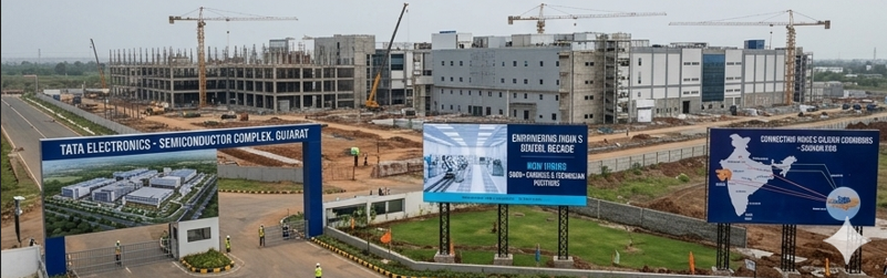
The Odisha plant is a centerpiece of the India Semiconductor Mission (ISM), which was launched with a ₹76,000 crore outlay. While the initial phase focused on attracting massive fabrication plants (like the Tata Group’s projects) and assembly units (like Micron), the government is now refining its strategy.
- Strategic Investment: This specific glass packaging project has garnered interest and funding from global giants like Intel and Lockheed Martin, highlighting its critical importance to both civilian tech and defense.
- The ISM 2.0 Shift: As the government prepares for a follow-up scheme with an estimated $11 billion outlay, the focus is expanding. Beyond just building “fabs,” ISM 2.0 is expected to support the ancillary ecosystem—chemicals, specialty gases, and design-linked incentives.
The “Why”: Strategic and Economic Imperatives of semiconductors
India’s focus on semiconductors is not merely an industrial goal; it is a matter of national security and economic future-proofing:
- Strategic Autonomy: In an era where chips power everything from smartphones to missile guidance systems, relying on a single geography (like Taiwan) is a risk. Developing domestic “fabs” ensures India’s defense and critical infrastructure cannot be “switched off” by external actors.
- The Electronics Boom: India is one of the world’s fastest-growing markets for electronics. By 2030, the domestic semiconductor market is expected to cross $110 billion. Producing chips locally helps reduce the massive import bill that currently drains foreign exchange reserves.
- Data Sovereignty: As AI models become the backbone of the economy, the physical hardware that processes this data becomes a vital asset. Controlling the hardware ensures that India’s data ecosystem remains secure and sovereign.
Current Challenges: The Hurdle to “Silicon Self-Reliance”
Despite the momentum of the India Semiconductor Mission (ISM), several structural bottlenecks persist that could slow down the “Bhubaneswar to Bangalore” tech corridor:
- Infrastructure Intensiveness: Semiconductor fabrication requires an ultra-stable environment. This includes uninterrupted 24/7 power supply and massive quantities of ultra-pure water—a single large “fab” can consume millions of gallons per day. Ensuring this at a global standard across Indian states remains a logistical challenge.
- The Talent-Experience Gap: While India has a world-class pool of chip designers (designing nearly 20% of the world’s chips), it lacks a workforce experienced in the physical manufacturing (fabrication) process. Transitioning from “designing on a screen” to “operating a multi-billion dollar cleanroom” requires a massive vocational shift.
- Supply Chain Dependencies: India currently lacks the ancillary ecosystem. The specialized gases, high-purity chemicals, and expensive photolithography equipment (like ASML’s EUV machines) must all be imported, making the local industry vulnerable to global geopolitical shifts.
Way Forward for India
To move from a “bet” to a “certainty,” India’s semiconductor policy must evolve from mere subsidies to ecosystem building:
- Strengthening ISM 2.0: The next phase of the mission must prioritize the ancillary supply chain. Providing incentives for companies that produce high-purity chemicals and gases within India will reduce the “Imported Inflation” of the manufacturing process.
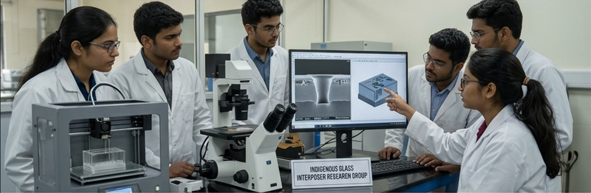
- The R&D-Academic Nexus: India should transform its premier institutes (IITs/NITs) into research hubs for Next-Gen materials like the 3D glass substrates mentioned in the Odisha project. This moves India from “assembling” tech to “owning” the intellectual property (IP).
- Global Collaborations (The Quad & Beyond): Leveraging partnerships like the iCET (Initiative on Critical and Emerging Technology) with the US can facilitate technology transfers and joint ventures, helping India bypass the decades-long learning curve faced by other nations.
Prelims Practise question:
Q. Under the India Semiconductor Mission (ISM), the government provides different layers of support. Which of the following is/are feature(s) of the revised ISM policy (ISM 2.0)?
1. Inclusion of incentives for ‘Design-Linked’ components specifically for domestic startups to own the intellectual property (IP).
2. Financial support for the manufacturing of “capital goods” and “specialty gases” required for the fabrication process.
3. A shift in focus from “mature nodes” (above 28nm) exclusively to “leading-edge nodes” (below 5nm) to compete with Taiwan.
Select the correct answer using the code given below:
A) 1 only
B) 1 and 2 only
C) 2 and 3 only
D) 1, 2, and 3
Answer : B (1 and 2 only)
Logic: ISM 2.0 specifically expanded to include ancillary industries like gases and capital goods (2) and continues to push Design-Linked Incentives (1). However, Statement 3 is incorrect because India is not exclusively focusing on <5nm nodes; it is still heavily incentivizing mature and trailing-edge nodes (like 28nm-40nm) which are used in automotive and industrial sectors.
Mains Practise question:
Discuss the socio-economic and logistical hurdles in making India a global semiconductor hub. How do the proposed changes in ‘ISM 2.0’ specifically address the deficiencies in the ancillary supply chain, such as specialty chemicals and ultra-pure water infrastructure?
(10 Marks, 150 Words)
- India’s Push Beyond E20 Fuel: Reasons, Pitfalls, and the Flex Fuel Future - June 15, 2026
- RBI’s Reviving of FCNR(B) Swap Scheme again in 2026 - June 15, 2026
- Modi’s France Visit & the 52nd G7 Summit - June 13, 2026

No Comments