


19 Sep Odisha’s 870-Acre Silicon Valley Hub: UPSC Exam Focus on Semiconductor Growth
✎ The Odisha Silicon Valley at Naraj exemplifies state-led industrial policy in India, combining fiscal incentives, infrastructure provision, and locational advantages to attract semiconductor and IT manufacturing under the India…
Subject Relevance — Where This Topic Fits
- GS Paper III — Indian Economy (Industrial Policy, Investment Promotion, Manufacturing Sector) | GS Paper III — Science & Technology (Semiconductor Industry, R&D, Supply Chain) | GS Paper III — Infrastructure (Industrial Corridors, Logistics, Connectivity) | GS Paper II — Federalism & Centre-State Relations (State-led Industrialisation, Investment Attraction)
- Prelims: Semiconductor Mission, Make in India, National Logistics Policy, Industrial Corridors, Special Economic Zones (SEZs), Ease of Doing Business, Maharatna/Navratna PSUs, PLI Schemes, Multimodal Connectivity, Water-intensive industries, Economic corridors, Bhubaneswar-Cuttack urban corridor
- Essay: India’s semiconductor self-reliance: Opportunities and challenges, Balancing industrial growth with environmental sustainability in India
Quick Revision: The Odisha Silicon Valley at Naraj exemplifies state-led industrial policy in India, combining fiscal incentives, infrastructure provision, and locational advantages to attract semiconductor and IT manufacturing under the India Semiconductor Mission framework.
Why is this in the news?
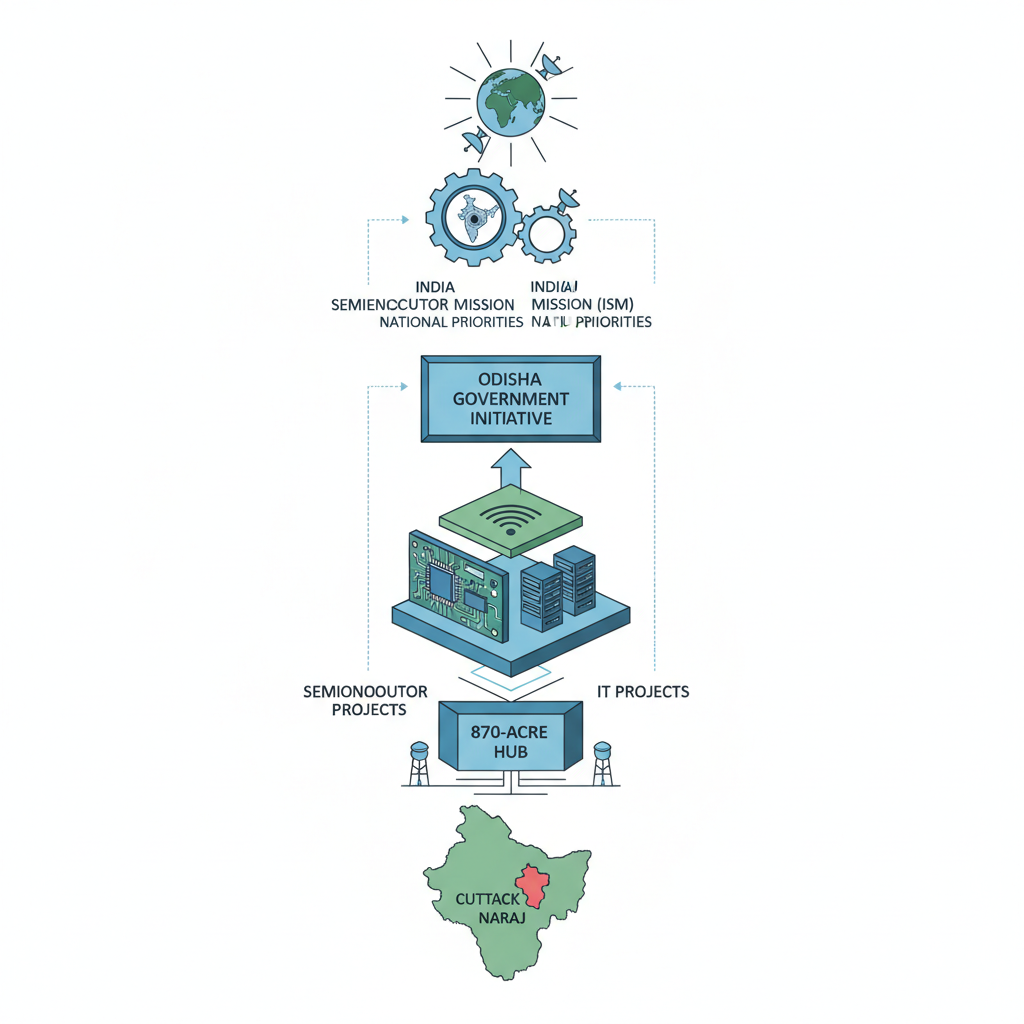
The Odisha government’s announcement of an 870-acre Silicon Valley hub in Naraj, Cuttack district, signifies a concerted effort to position the state as a strategic node in India’s semiconductor and IT manufacturing ecosystem. This initiative aligns with national priorities under the India Semiconductor Mission (ISM) and underscores the role of state governments in industrial policy, investment promotion, and infrastructure development. The project’s emphasis on connectivity, water resources, and fiscal incentives reflects contemporary policy tools used to attract high-technology industries.
Background
- The semiconductor industry is a critical component of the global electronics value chain, with applications spanning consumer electronics, automotive, defence, and telecommunications.
- India’s semiconductor ecosystem has historically been import-dependent, with over 90% of its semiconductor requirements met through imports, highlighting the need for domestic manufacturing capabilities.
- The Government of India launched the India Semiconductor Mission (ISM) in December 2021 with an outlay of ₹76,000 crore, aiming to establish India as a global hub for semiconductor design, manufacturing, and supply chain resilience.
- State governments play a pivotal role in industrialisation through policy frameworks, land acquisition, infrastructure provision, and fiscal incentives, often in collaboration with central schemes like PLI (Production-Linked Incentive).
- Odisha’s strategic location along the eastern coast provides access to major ports (Paradip, Dhamra) and connectivity to national highways (NH-16, NH-516), facilitating multimodal logistics for industrial supply chains.
- The Bhubaneswar-Cuttack urban corridor is a key economic region in Odisha, with established industrial infrastructure and a skilled workforce, making it conducive for high-technology industries.
What is the Odisha Silicon Valley at Naraj?
- A proposed 870-acre industrial hub in Naraj, Cuttack district, designated for semiconductor fabrication, electronics manufacturing, and IT services, with a focus on integrating the entire value chain from design to assembly.
- The project aims to leverage Odisha’s locational advantages, including proximity to the Mahanadi River for water supply, connectivity to ports (Paradip, Dhamra), and access to the Bhubaneswar-Cuttack urban corridor for skilled manpower and logistics.
- The hub is envisaged as a self-contained ecosystem with dedicated infrastructure for power, water, waste management, and residential facilities to support a high-technology workforce.
- The state government has extended additional fiscal support of 25% to projects approved under the India Semiconductor Mission (ISM), covering semiconductor equipment manufacturing, semiconductor-grade gases, raw materials, and supply-chain segments.
- Policy incentives include support for engineer relocation, manpower skilling, internships, international patents, and R&D, aligning with national priorities for technology-driven industrialisation.
- Investment proposals worth approximately ₹23,600 crore have been received, with the potential to generate 6,100 employment opportunities, indicating strong industry interest in the project.
- The initiative reflects a broader trend of state-led industrialisation in India, where subnational governments are actively competing to attract high-value manufacturing through targeted policies and infrastructure development.
- The project’s success will depend on coordination between the state government, central agencies (e.g., MeitY, DPIIT), and private investors, as well as the timely execution of infrastructure and regulatory clearances.
Key Features
| Feature | Significance |
|---|---|
| 870-acre integrated hub | Provides contiguous land for semiconductor fabrication, assembly, and IT projects under one administrative framework. |
| Proximity to Mahanadi River | Ensures reliable water supply for high-purity semiconductor manufacturing processes. |
| Multimodal connectivity | Links to Cuttack–Bhubaneswar corridor, Paradip and Dhamra ports, and national highways for logistics efficiency. |
| Fiscal incentives (25% additional support) | Enhances competitiveness for semiconductor equipment, gases, and supply-chain segments under India Semiconductor Mission. |
| Investment proposals worth ₹23,600 crore | Demonstrates investor confidence and potential to catalyse ecosystem growth. |
Why it Matters
Economic Significance
- Establishes Odisha as a strategic node in India’s semiconductor and electronics value chain, reducing import dependence.
- Generates 6,100 direct employment opportunities, with potential for indirect job creation in ancillary industries.
- Boosts local GDP through high-value manufacturing and services, aligning with ‘Atmanirbhar Bharat’ objectives.
Strategic Significance
- Reduces supply chain vulnerabilities by diversifying semiconductor manufacturing beyond existing hubs (Gujarat, Karnataka, Tamil Nadu).
- Leverages Odisha’s coastal proximity for export-oriented production, enhancing India’s global semiconductor competitiveness.
- Supports India’s semiconductor mission (2021) by providing infrastructure for fabrication, assembly, testing, marking, and packaging (ATMP).
Industrial Infrastructure
- Creates a dedicated ecosystem with shared utilities (power, water, waste management) to reduce per-unit costs for investors.
- Facilitates clustering of semiconductor suppliers, R&D centres, and skilled workforce under one administrative umbrella.
- Enables integration with existing industrial corridors (e.g., Bhubaneswar–Cuttack) for synergies in logistics and labour.
Challenges
1. Land Acquisition and Rehabilitation
- Large-scale land acquisition may face resistance from local communities, requiring transparent compensation and resettlement policies.
- Ensuring environmental compliance for 870 acres, including impact assessments for water usage and ecosystem disruption.
UPSC Link: Land Acquisition Act, 2013 (LARR Act)
2. Water and Power Infrastructure
- Semiconductor fabrication demands high-purity water and uninterrupted power; Odisha must ensure 24/7 supply with zero tolerance for outages.
- Coal-based power may conflict with decarbonisation goals; transition to renewable energy sources (e.g., solar) is essential.
UPSC Link: National Water Policy 2012
3. Skilled Workforce Development
- Semiconductor manufacturing requires specialised skills; Odisha must collaborate with IITs, NITs, and vocational institutes for curriculum alignment.
- Attracting and retaining talent from other states may necessitate housing, education, and healthcare incentives.
UPSC Link: National Skill Development Mission
4. Global Supply Chain Integration
- Competing with established hubs (e.g., TSMC in Taiwan, Intel in the US) requires seamless integration into global semiconductor supply chains.
- Ensuring intellectual property protection and cybersecurity for foreign investors.
UPSC Link: World Trade Organization (WTO) Agreements
5. Policy Consistency and Ease of Doing Business
- Long-term policy stability is critical to prevent investor flight; Odisha must align with central schemes (e.g., PLI for semiconductors).
- Streamlining approvals (environmental, labour, industrial) to reduce project timelines and costs.
UPSC Link: Ease of Doing Business (EODB) Index
Challenges — UPSC Perspective
| Issue | Concern |
|---|---|
| Land acquisition delays | Potential litigation and community opposition may stall project timelines. |
| Water scarcity risks | Semiconductor plants require 10–15 million litres/day; Mahanadi’s seasonal variability must be managed. |
| Power reliability | Grid instability or coal shortages could disrupt fabrication processes, leading to financial losses. |
| Talent retention | High attrition rates in semiconductor roles may necessitate competitive compensation and training programs. |
| Regulatory hurdles | Overlapping approvals from state and central agencies could delay clearances. |
| Environmental compliance | Strict norms for effluent treatment and carbon footprint may increase operational costs. |
Government Initiatives — Must-Memorise for Prelims
- India Semiconductor Mission (ISM) 2021
Way Forward
- Constitute a dedicated project management unit (PMU) to oversee land acquisition, environmental clearances, and utility infrastructure.
- Collaborate with central agencies (e.g., MeitY, NITI Aayog) to align state policies with ISM’s PLI scheme and fiscal incentives.
- Invest in vocational training programs in partnership with semiconductor firms to develop a local talent pipeline.
- Develop a water management plan integrating rainwater harvesting, treated wastewater reuse, and Mahanadi basin sustainability studies.
- Establish a single-window clearance system to streamline approvals for investors, reducing project gestation periods.
- Create a green energy corridor with solar/wind power to meet semiconductor plants’ decarbonisation targets.
- Launch a global investor outreach program targeting semiconductor firms in Japan, Taiwan, and the EU to secure anchor investments.
- Monitor and publish quarterly progress reports to maintain transparency and investor confidence.
UPSC Value Addition
Keywords for Mains Answer-Writing
Semiconductor ecosystem · Odisha Silicon Valley · Naraj Cuttack · India Semiconductor Mission · semiconductor policy · semiconductor supply chain · semiconductor fabrication · semiconductor manufacturing · industrial corridors · multimodal connectivity · semiconductor value chain · semiconductor-grade materials · semiconductor employment generation · semiconductor fiscal incentives · semiconductor R&D
Concept Flow
Odisha’s strategic location and infrastructure gaps → State government announces 870-acre Silicon Valley hub → Investor proposals worth ₹23,600 crore received → Semiconductor fabrication and IT projects planned → Employment generation and GDP growth anticipated → Challenges in land, water, and skill development emerge → Policy interventions and infrastructure upgrades required → Long-term integration into India’s semiconductor ecosystem.
Prelims Practice Questions
Q1. Consider the following statements regarding the India Semiconductor Mission (ISM):
1. The ISM is a central sector scheme aimed at developing a sustainable semiconductor and display ecosystem in India.
2. The ISM provides fiscal support of up to 50% of the project cost for semiconductor fabrication units.
3. The ISM includes provisions for support in semiconductor equipment manufacturing and supply-chain segments.
4. The ISM mandates state governments to provide additional fiscal incentives beyond the central scheme.
How many of the above statements are correct?
- Only one
- Only two
- Only three
- All four
Answer: Only three — Statements 1 and 3 are correct as per the ISM framework. Statement 2 is incorrect; fiscal support for semiconductor fabrication units is up to 50% of capital expenditure, not project cost. Statement 4 is incorrect; state governments may provide additional incentives but it is not mandated by ISM.
Q2. Assertion (A): The Odisha Silicon Valley project in Naraj, Cuttack, is strategically located near the Mahanadi River to address water requirements for semiconductor fabrication facilities.
Reason (R): Semiconductor fabrication units require large quantities of ultra-pure water, and proximity to a major river ensures a reliable water supply for industrial processes.
In the context of the above two statements, which of the following is correct?
- Both A and R are true, and R is the correct explanation of A
- Both A and R are true, but R is not the correct explanation of A
- A is true but R is false
- A is false but R is true
Answer: Both A and R are true, and R is the correct explanation of A — Both A and R are true. Semiconductor fabrication units indeed require substantial quantities of ultra-pure water, and the Mahanadi River provides a significant locational advantage for water supply. R correctly explains A.
Q3. Match the following pairs related to semiconductor manufacturing and their descriptions:
Column I
1. Semiconductor fabrication facility
2. Semiconductor assembly unit
3. Semiconductor-grade materials
4. Semiconductor supply chain
Column II
A. Involves packaging and testing of semiconductor devices
B. Produces integrated circuits on silicon wafers
C. Includes raw materials like silicon ingots, chemicals, and gases
D. Encompasses the entire ecosystem from raw materials to end products
Select the correct match:
- 1-B, 2-A, 3-C, 4-D
- 1-A, 2-B, 3-C, 4-D
- 1-B, 2-A, 3-D, 4-C
- 1-A, 2-B, 3-D, 4-C
Answer: 1-B, 2-A, 3-C, 4-D — 1-B: Semiconductor fabrication facilities produce integrated circuits on silicon wafers. 2-A: Assembly units involve packaging and testing. 3-C: Semiconductor-grade materials include raw materials like silicon ingots and chemicals. 4-D: The supply chain encompasses the entire ecosystem.
Mains Practice Question
✍ The establishment of the Odisha Silicon Valley in Naraj, Cuttack, represents a significant step towards India’s self-reliance in the semiconductor sector. Critically examine the strategic, economic, and infrastructural dimensions of this initiative, with reference to the India Semiconductor Mission and contemporary global semiconductor supply chain dynamics. (15 Marks)
Approach: A full answer must cover the following dimensions:
1. **Strategic Dimensions**:
– Location advantages: proximity to Mahanadi River for water, connectivity to Cuttack–Bhubaneswar corridor, multimodal access to Paradip and Dhamra ports, and key national highways.
– Strategic role in the semiconductor supply chain: potential hub for fabrication, assembly, and allied industries.
– Alignment with national objectives: contribution to India’s semiconductor self-reliance (Atmanirbhar Bharat) and reduction of import dependence.
2. **Economic Dimensions**:
– Investment proposals: Rs 23,600 crore and potential to generate 6,100 employment opportunities.
– Fiscal incentives: 25% additional support by Odisha for ISM-approved projects in semiconductor equipment manufacturing, semiconductor-grade gases, raw materials, and supply-chain segments.
– Policy framework: support for engineer relocation, manpower skilling, internships, international patents, and R&D.
3. **Infrastructural Dimensions**:
– Multimodal connectivity: seamless integration with urban corridors, ports, and highways.
– Industrial ecosystem: potential to attract global semiconductor manufacturers (e.g., delegations from Japan, Sweden, and Taiwan).
– Water and power infrastructure: reliance on Mahanadi River for industrial water and existing power infrastructure.
4. **Contemporary Global Context**:
– Semiconductor supply chain dynamics: global shifts post-COVID-19 and geopolitical tensions (e.g., US-China trade war, CHIPS Act).
– India’s position: challenges in competing with established hubs (e.g., Taiwan, South Korea, USA) and opportunities in diversifying supply chains.
5. **Critical Examination**:
– Challenges: high capital expenditure, technological complexity, competition from established hubs, and need for sustained policy support.
– Sustainability: ensuring long-term viability through continuous innovation, R&D investment, and skill development.
– Balancing act: between attracting global investment and ensuring local value addition and employment generation.
6. **Conclusion**:
– Summarise the potential of Odisha Silicon Valley as a catalyst for India’s semiconductor ecosystem.
– Highlight the need for coordinated action among central and state governments, industry, and academia to realise its full potential.
Source: The Hindu
Odisha PCS (OPSC (OAS)) — State PCS Practice
Prelims: The Odisha government has proposed to set up a 870-acre ‘Silicon Valley’ hub in Naraj, Cuttack, primarily for which of the following sectors?
- Semiconductor and IT projects
- Agriculture and food processing
- Textile and garment manufacturing
- Mining and mineral processing
Answer: Semiconductor and IT projects — The proposed 870-acre ‘Silicon Valley’ hub in Naraj, Cuttack is aimed at fostering semiconductor and IT projects as part of Odisha’s industrial development strategy.
Mains: Discuss the strategic significance of the proposed 870-acre ‘Silicon Valley’ hub in Naraj, Cuttack for Odisha’s economy. Highlight its potential impact on employment generation, technological advancement, and industrial diversification in the state.
Generated by AanyaAi for educational purpose.
Related guides on our sites
- Current affairs for upsc 2026
- How to prepare for GS paper 1 for UPSC CSE mains exam
- Best UPSC coaching for IFOS exam
- Best mentorship programme for upsc

- Odisha’s 870-Acre Silicon Valley Hub: UPSC Exam Focus on Semiconductor Growth - September 19, 2026
- यूपीएससी तैयारी: आरबीआई द्वारा 91, 182 और 364 दिनों के ट्रेजरी बिलों की नीलामी - September 19, 2026
- RBI to Auction ₹24,000 Crore T-Bills: Key Dates & Process for UPSC Aspirants - September 19, 2026
No Comments