


08 Aug Bengaluru INDIA NANO 2026: Semiconductor Ecosystem & Nano Innovations Highlighted
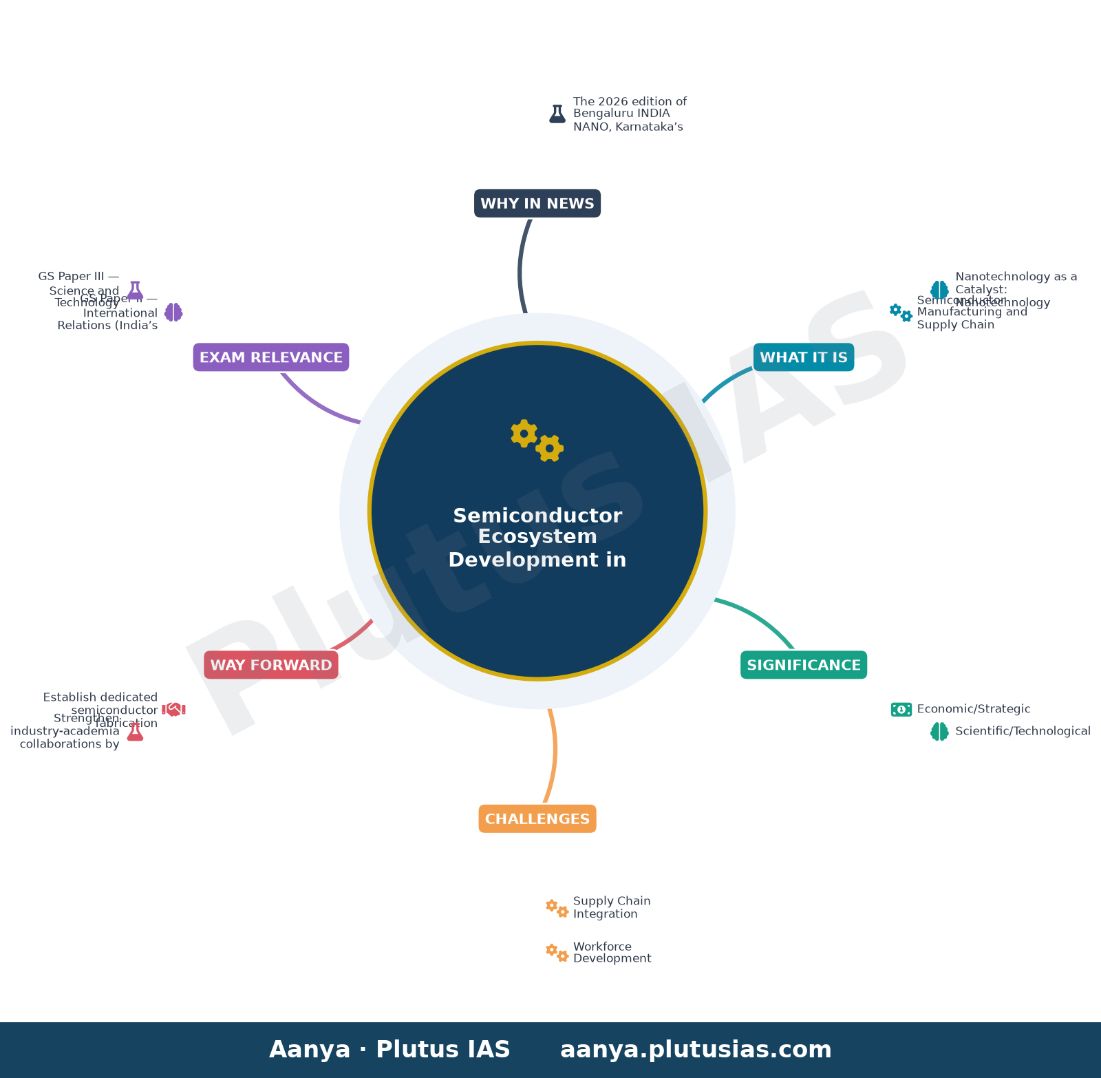
✎ India’s semiconductor ecosystem development hinges on integrating supply chains, fostering indigenous innovation in nanotechnology, and leveraging public-private partnerships to achieve self-reliance in critical technologies.
Subject Relevance — Where This Topic Fits
- GS Paper II — International Relations (India’s role in global technology supply chains) | GS Paper III — Science and Technology (Semiconductor manufacturing, nanotechnology, and R&D ecosystem) | GS Paper III — Economy (Industrial policy, Make in India, and sectoral competitiveness)
- Prelims: Semiconductor Mission India, Nanotechnology Policy of India, PLI Scheme for Semiconductors, Karnataka’s IT-BT Policy, Bharat Ratna C.N.R. Rao, Lam Research, KSTePS, Hydrodynamic Cavitation Nanobubble Technology
- Essay: The Role of Science and Technology in India’s Development: From Laboratory to Last-Mile Transformation, Global Supply Chain Resilience and India’s Strategic Position in Semiconductor Manufacturing
Quick Revision: India’s semiconductor ecosystem development hinges on integrating supply chains, fostering indigenous innovation in nanotechnology, and leveraging public-private partnerships to achieve self-reliance in critical technologies.
Why is this in the news?
The 2026 edition of Bengaluru INDIA NANO, Karnataka’s flagship international nanotechnology conference, has brought the semiconductor ecosystem into sharp focus by highlighting India’s strategic ambitions in semiconductor manufacturing, advanced R&D in nanotechnology, and the integration of supply chains. The event underscores the state’s proactive role in fostering innovation through initiatives like the Karnataka Science and Technology Promotion Society (KSTePS) and the recognition of indigenous technologies such as hydrodynamic-cavitation nanobubble systems. This aligns with national policies aimed at reducing import dependence in critical technologies.
Background
- The global semiconductor industry is projected to exceed USD 1 trillion by 2030, with demand driven by AI, IoT, and 5G/6G technologies, making self-reliance in this sector a geopolitical and economic imperative for India.
- India’s Semiconductor Mission (2021), with an outlay of INR 76,000 crore, aims to position the country as a global hub for semiconductor design, manufacturing, and assembly, testing, and packaging (ATMP).
- Karnataka, home to Bengaluru—the ‘Silicon Valley of India’—hosts over 40% of India’s IT workforce and is a critical node in the semiconductor supply chain, particularly for design and R&D.
Semiconductor Ecosystem and Nanotechnology: Key Dimensions of India’s Technological Ambition
- Semiconductor Manufacturing and Supply Chain Integration: Semiconductors are the backbone of modern electronics, with applications spanning computing, telecommunications, automotive, and defence. India’s strategy focuses on end-to-end ecosystem development, including design, fabrication, assembly, testing, and packaging (ATMP), to reduce import dependence and enhance value addition.
- Nanotechnology as a Catalyst: Nanotechnology enables the miniaturization of semiconductor components, advanced materials (e.g., graphene, quantum dots), and energy-efficient devices. The Bengaluru INDIA NANO event highlights Karnataka’s leadership in this domain through R&D, startups, and industry-academia collaboration.
- Indigenous Innovation in Water Treatment: The award to Prasinos Tech Innovations for hydrodynamic-cavitation nanobubble technology demonstrates India’s capability in developing cutting-edge solutions for water purification and ecosystem restoration, which are critical for sustainable development and rural resilience.
- Research and Human Capital Development: The Karnataka DST Nanoscience Fellowship Awardees 2026 reflect the state’s commitment to nurturing talent in advanced research, with awardees from premier institutions like IISc Bengaluru, JNCASR, IACS Kolkata, INST Mohali, and IIT Delhi, ensuring a pipeline of skilled researchers.
- Public-Private Partnerships: Events like Bengaluru INDIA NANO facilitate collaboration between government agencies (e.g., KSTePS, DST), academia (e.g., IISc, JNCASR), and industry leaders (e.g., Lam Research), creating an ecosystem that bridges the gap between lab-scale research and commercial deployment.
- Policy Support and Incentives: The Semiconductor Mission provides financial and regulatory support to attract investment.
- Global Positioning and Geopolitical Imperatives: India’s push for semiconductor self-reliance is part of a broader strategy to diversify global supply chains, reduce dependence on China and other single-source suppliers, and align with allies like the US and EU in critical technology alliances.
Key Features
| Feature | Significance |
|---|---|
| Bengaluru INDIA NANO 2026 | A premier international platform for nanotechnology and semiconductor research, fostering collaboration between academia, industry, and government to advance India’s scientific and industrial capabilities. |
| C.N.R. Rao Felicitation | Recognizes the foundational contributions of India’s leading scientist in nanoscience, reinforcing the nation’s commitment to scientific excellence and research-led innovation. |
| Hydrodynamic-Cavitation Nanobubble Technology | Indigenous innovation in water treatment and ecosystem restoration, demonstrating India’s capacity for cutting-edge research translating to societal impact. |
| Karnataka DST Nanoscience Fellowships | Institutional support for PhD scholars in nanoscience, ensuring sustained human resource development in critical STEM fields. |
| Lam Research India’s Semiconductor Ecosystem Vision | Highlights India’s strategic focus on integrating supply chains, advanced engineering, and workforce development to capture a share of the global semiconductor market. |
Why it Matters
Economic/Strategic
- India’s semiconductor ecosystem is positioned as a critical component of its economic growth and self-reliance (Atmanirbhar Bharat) agenda, with Bengaluru emerging as a global hub for nanotechnology and semiconductor innovation.
- The integration of advanced engineering, research, and skilled workforce development is essential to reduce import dependence and enhance India’s competitiveness in high-technology manufacturing.
- The global semiconductor market, projected to exceed USD 1 trillion by 2030, presents a substantial opportunity for India to establish itself as a key player in the supply chain.
Scientific/Technological
- Nanoscience and nanotechnology are pivotal to India’s future in sectors such as healthcare, energy, and environmental sustainability, with applications ranging from water purification to advanced materials.
- Indigenous innovations like hydrodynamic-cavitation nanobubble technology demonstrate India’s capability to develop homegrown solutions for pressing national challenges.
- The recognition of C.N.R. Rao underscores the importance of foundational research in driving applied technological advancements.
Social/Institutional
- The emphasis on taking science beyond laboratories to underserved communities reflects a commitment to inclusive development and equitable access to technological benefits.
- Institutional fellowships and awards incentivize young researchers, fostering a culture of innovation and scientific temper in India.
- Conferences like Bengaluru INDIA NANO serve as bridges between academia, industry, and policymakers, facilitating knowledge exchange and collaborative problem-solving.
Challenges
1. Supply Chain Integration
- India lacks a fully integrated semiconductor supply chain, with critical gaps in raw material availability, manufacturing infrastructure, and advanced packaging capabilities.
- Dependence on imports for key semiconductor components (e.g., wafers, photoresists) exposes the industry to geopolitical and economic vulnerabilities.
- The need to align with global standards while developing domestic capabilities poses a significant challenge in scaling up production.
UPSC Link: GS3: Science & Technology – Developments and their Applications
2. Workforce Development
- India faces a shortage of skilled professionals in semiconductor design, nanotechnology, and advanced manufacturing, necessitating targeted education and training programs.
- The gap between academic research and industry requirements requires reforms in curricula and stronger industry-academia collaborations.
- Retention of talent in India remains a challenge due to competition from global firms and better remuneration abroad.
UPSC Link: GS3: Human Resource Development
3. Research-to-Commercialization Gap
- While India has strong research institutions (e.g., IISc, JNCASR), translating academic innovations into commercial products remains a persistent hurdle.
- Insufficient funding for prototype development, regulatory bottlenecks, and risk-averse investment climate delay the commercialization of indigenous technologies.
- The lack of venture capital and angel investment ecosystems in deep-tech sectors like semiconductors exacerbates this challenge.
UPSC Link: GS3: Science & Technology – Technology Missions
4. Infrastructure and Policy Gaps
- India lacks dedicated semiconductor fabrication facilities (fabs) and advanced testing laboratories, which are prerequisites for a robust ecosystem.
- Bureaucratic delays, regulatory complexities, and inconsistent policy frameworks hinder the ease of doing business in the sector.
- State-level initiatives (e.g., Karnataka’s policies) must be complemented by cohesive national strategies to avoid fragmentation.
UPSC Link: GS2: Government Policies & Interventions
5. Global Competition
- India competes with established semiconductor hubs like Taiwan, South Korea, and the US, which have mature ecosystems and state-backed incentives.
- Geopolitical tensions (e.g., US-China trade war) and export controls (e.g., semiconductor equipment restrictions) pose additional barriers to India’s entry into global value chains.
- The need to align with global standards (e.g., ISO, SEMI) while developing domestic capabilities adds complexity.
UPSC Link: GS2: Bilateral & Multilateral Groupings
Challenges — UPSC Perspective
| Issue | Concern |
|---|---|
| Semiconductor Supply Chain | Dependence on imports for critical components and lack of domestic manufacturing infrastructure. |
| Skilled Workforce Shortage | Inadequate training programs and brain drain to foreign firms hinder sector growth. |
| Research Commercialization | Gap between academic innovation and industry adoption due to funding and regulatory barriers. |
| Infrastructure Deficit | Absence of fabs and advanced testing facilities limits self-reliance in semiconductor production. |
| Policy Fragmentation | Inconsistent state and central policies create uncertainty for investors and innovators. |
| Global Competition | Established semiconductor hubs and geopolitical constraints pose entry barriers for India. |
Way Forward
- Establish dedicated semiconductor fabrication facilities (fabs) through public-private partnerships, leveraging global expertise and state incentives.
- Strengthen industry-academia collaborations by funding joint research projects and establishing technology transfer offices in premier institutions.
- Develop targeted skill development programs in collaboration with semiconductor firms (e.g., Lam Research, Intel) to bridge the workforce gap.
- Create a national semiconductor mission with clear timelines, funding mechanisms, and regulatory frameworks to ensure coherence across states.
- Incentivize venture capital and angel investment in deep-tech sectors through tax breaks, grants, and incubation support.
- Enhance public-private partnerships to accelerate the commercialization of indigenous technologies (e.g., hydrodynamic-cavitation nanobubble systems).
- Align India’s semiconductor standards with global benchmarks to facilitate integration into international supply chains.
- Promote state-level initiatives (e.g., Karnataka’s policies) while ensuring alignment with a unified national strategy to avoid fragmentation.
UPSC Value Addition
Keywords for Mains Answer-Writing
Semiconductor ecosystem · Nanotechnology · Bengaluru India Nano · C.N.R. Rao · Semiconductor supply chain resilience · Karnataka’s STI policy · KSTePS fellowships · Lam Research India · Indigenous nanobubble technology · Global semiconductor industry · Science and technology integration · Rural science outreach
Concept Flow
Global semiconductor demand surge → India’s Atmanirbhar Bharat initiative → Focus on Bengaluru as a nanotechnology hub → Bengaluru INDIA NANO 2026 event → Recognition of C.N.R. Rao and indigenous innovations → Highlighting supply chain, workforce, and research challenges → Policy and institutional responses → Way forward for ecosystem development
Prelims Practice Questions
Q1. Consider the following statements regarding the Bengaluru INDIA NANO programme:
1. The 2026 edition of the programme was inaugurated by Bharat Ratna C.N.R. Rao.
2. The programme has been felicitated for its role in advancing nanoscience research in India.
3. The Karnataka DST Nanoscience Fellowship is awarded to support PhD scholars in advanced research in nanoscience and engineering.
How many of the above statements are correct?
- Only one
- Only two
- All three
- None
Answer: All three — Statements 2 and 3 are correct. Statement 1 is incorrect as C.N.R. Rao was felicitated during the programme, but he did not inaugurate it.
Q2. Assertion (A): India’s opportunity in the global semiconductor industry lies in building a resilient semiconductor ecosystem that integrates supply chains, advanced engineering, research, and a skilled workforce.
Reason (R): The Lam Research India Corporate Vice President and Managing Director, Rangesh Raghavan, highlighted this during the Bengaluru INDIA NANO 2026 programme.
Options:
A. Both A and R are true, and R is the correct explanation of A.
B. Both A and R are true, but R is not the correct explanation of A.
C. A is true, but R is false.
D. A is false, but R is true.
Answer: ? — Both the Assertion (A) and Reason (R) are true, and R correctly explains A as it directly quotes Raghavan’s statement during the programme.
Q3. Match the following awardees of the Karnataka DST Nanoscience Fellowship Awardees 2026 with their respective institutions:
Column I (Awardees) | Column II (Institutions)
1. Pritam Pal | A. IISc Bengaluru
2. Debmalya Mukhopadhyay | B. JNCASR Bengaluru
3. Souvik Banerjee | C. IACS Kolkata
4. Alisha Rohal | D. INST Mohali
5. Sudip Naskar | E. IIT Delhi
- 1-A, 2-B, 3-C, 4-D, 5-E
- 1-B, 2-A, 3-C, 4-D, 5-E
- 1-A, 2-B, 3-D, 4-C, 5-E
- 1-E, 2-B, 3-C, 4-D, 5-A
Answer: 1-A, 2-B, 3-C, 4-D, 5-E — The correct matches are: Pritam Pal (IISc Bengaluru), Debmalya Mukhopadhyay (JNCASR Bengaluru), Souvik Banerjee (IACS Kolkata), Alisha Rohal (INST Mohali), and Sudip Naskar (INST Mohali). Snehraj Gaur (IIT Delhi) was also mentioned but not part of the matching options.
Mains Practice Question
✍ The development of a resilient semiconductor ecosystem in India is contingent upon the integration of supply chains, advanced engineering, research, and a skilled workforce. Critically examine this proposition in the context of India’s current efforts, with reference to recent initiatives and challenges. (15 Marks)
Approach: MODEL-ANSWER SKELETON:
1. **Introduction**: Define the semiconductor ecosystem and its critical components (supply chains, R&D, skilled workforce, manufacturing).
2. **India’s Current Efforts**:
– **Semiconductor Mission**: Outline the India Semiconductor Mission (ISM) and its objectives (e.g., fiscal support, PLI schemes, design-linked incentive schemes).
– **Global Partnerships**: Mention collaborations with firms like Lam Research, Micron, and Tata Electronics for fab establishment and supply chain integration.
– **Research and Innovation**: Highlight initiatives like Bengaluru India Nano, KSTePS fellowships, and indigenous technologies (e.g., Prasinos Tech’s nanobubble technology).
3. **Challenges**:
– **Supply Chain Vulnerabilities**: Dependence on imports for critical materials (e.g., silicon wafers, photoresists).
– **Skilled Workforce Gap**: Shortage of semiconductor-specific engineers and technicians; need for STEM education reforms.
– **Infrastructure Bottlenecks**: High capital costs, land acquisition, and power/water availability for semiconductor fabs.
– **Geopolitical Risks**: Over-reliance on a few countries (e.g., China, Taiwan) for critical inputs.
4. **Comparative Perspective**: Contrast India’s progress with global leaders (e.g., US CHIPS Act, EU Chips Act, China’s semiconductor push).
5. **Way Forward**:
– Strengthen public-private partnerships and academia-industry linkages.
– Invest in R&D hubs (e.g., IISc, IITs) and upskilling programmes.
– Diversify supply chains and reduce import dependence through domestic production.
6. **Conclusion**: Reiterate the need for a holistic, long-term strategy to build a resilient semiconductor ecosystem, balancing immediate gains with sustainable growth.
Source: The Hindu
Generated by AanyaAi for educational purpose.

- KWML’s Feasibility Reports for Water Metro in 18 Cities: UPSC & PCS Insights - October 3, 2026
- ओडिशा में वन्यजीव अनुसंधान अनुदान कार्यक्रम शुरू, सिमिलिपाल में 300 कैमरे और बढ़ेंगे - October 3, 2026
- India Summons Pakistan High Commission Official Over Violation - October 3, 2026
No Comments