


08 Aug Bengaluru INDIA NANO 2026: Semiconductor & Nanoscience Ecosystem Boost
✎ India’s Semiconductor Mission seeks to reduce import dependence by leveraging domestic innovation in nanotechnology and state-led policies, with Karnataka’s Bengaluru India Nano serving as a critical platform for integrating…
Subject Relevance — Where This Topic Fits
- GS Paper II — Global Groupings and Agreements Involving India and/or Affecting India’s Interests | GS Paper III — Effects of Liberalisation on the Economy, Changes in Industrial Policy and Their Effects on Industrial Growth | GS Paper III — Science and Technology — Developments and Their Applications and Effects in Everyday Life | GS Paper III — Awareness in the Fields of IT, Space, Computers, Robotics, Nano-Technology, Bio-Technology and Issues Relating to Intellectual Property Rights
- Prelims: Semiconductor Mission India (SMI), Modified Special Incentive Package Scheme (M-SIPS), Production-Linked Incentive (PLI) Scheme for Semiconductors, Atomic Layer Deposition (ALD), Hydrodynamic Cavitation, Nanobubbles, Karnataka Science and Technology Promotion Society (KSTePS), Bengaluru India Nano
- Essay: Technological Sovereignty and India’s Path to Self-Reliance in Critical Technologies, The Role of State Governments in Fostering Innovation Ecosystems: A Case Study of Karnataka
Quick Revision: India’s Semiconductor Mission seeks to reduce import dependence by leveraging domestic innovation in nanotechnology and state-led policies, with Karnataka’s Bengaluru India Nano serving as a critical platform for integrating research, industry, and policy.
Why is this in the news?
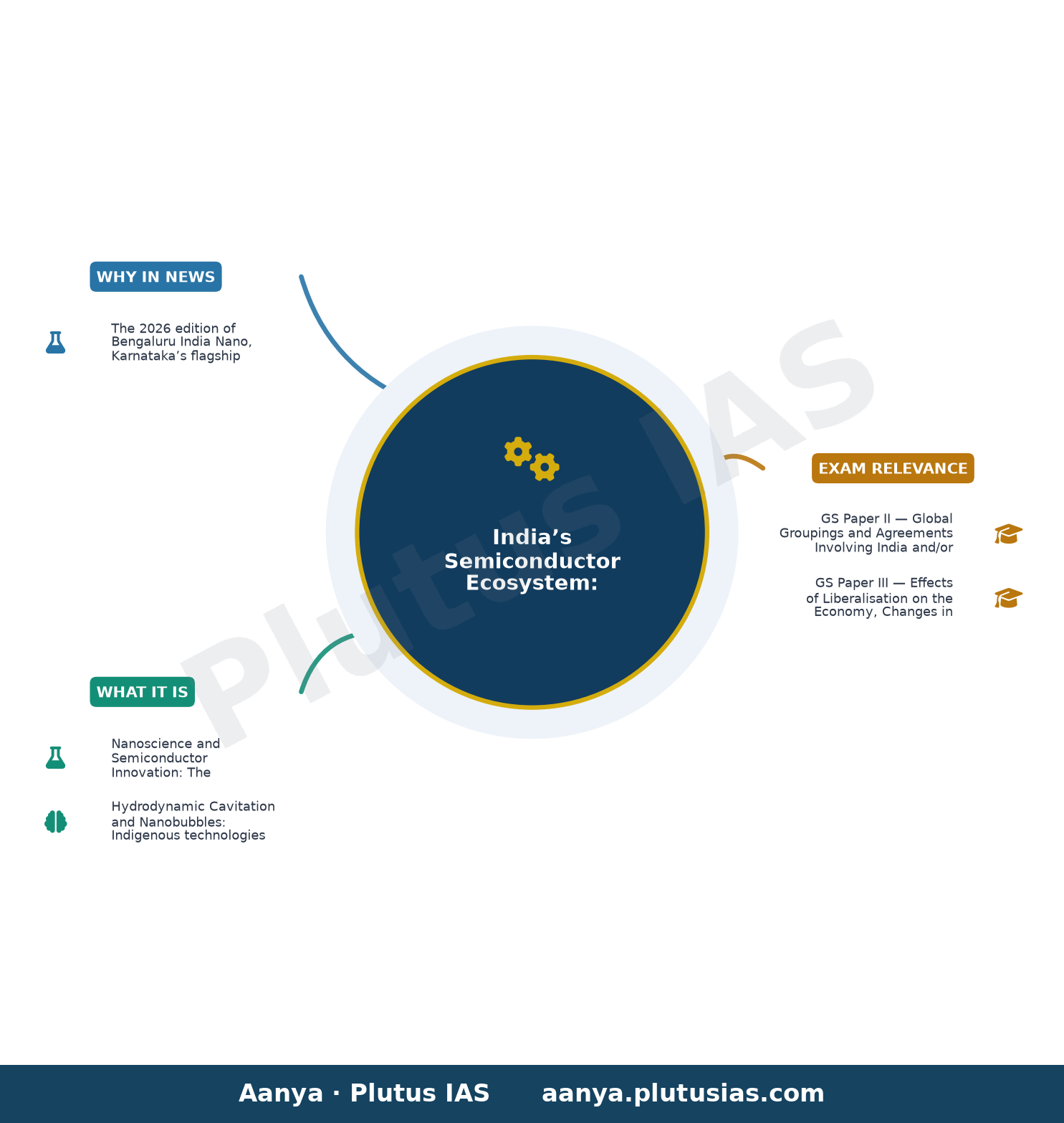
The 2026 edition of Bengaluru India Nano, Karnataka’s flagship international nanotechnology conference, has brought the semiconductor ecosystem into sharp focus by highlighting India’s strategic ambitions in semiconductor manufacturing and the integration of nanoscience innovations. The event underscores Karnataka’s proactive role in fostering a resilient semiconductor value chain through policy initiatives, research fellowships, and industry-academia collaboration, while also honouring Bharat Ratna C.N.R. Rao for his foundational contributions to nanoscience and science outreach.
Background
- India’s semiconductor demand is driven by domestic consumption in electronics, automotive, and defence sectors, as well as export opportunities in the global value chain, particularly for mature nodes (28nm and above).
- Nanoscience and nanotechnology are increasingly recognised as critical enablers for semiconductor innovation, particularly in materials science, energy efficiency, and advanced manufacturing processes like nanoscale lithography.
Semiconductor Ecosystem in India: Strategic Framework, Nanoscience Integration, and Karnataka’s Role
- Nanoscience and Semiconductor Innovation: The integration of nanotechnology in semiconductor manufacturing enables advancements in materials like graphene, carbon nanotubes, and quantum dots, which enhance performance, reduce power consumption, and enable miniaturisation of devices.
- Hydrodynamic Cavitation and Nanobubbles: Indigenous technologies like those developed by Prasinos Tech Innovations utilise hydrodynamic cavitation to generate nanobubbles for water treatment and ecosystem restoration, demonstrating the potential of nanotechnology in addressing environmental challenges while supporting semiconductor manufacturing processes.
- Karnataka Science and Technology Promotion Society (KSTePS): A state nodal agency under the Department of Science and Technology, Karnataka, which supports research fellowships, innovation awards, and industry-academia collaborations to foster a robust R&D ecosystem in nanoscience and semiconductor technologies.
Key Features
| Feature | Significance |
|---|---|
| Bengaluru INDIA NANO 2026 | An annual international conference and exhibition in Karnataka, serving as a pivotal platform for advancing nanotechnology, semiconductor research, and industry-academia collaboration in India. |
| Felicitation of C.N.R. Rao | A tribute to India’s eminent scientist for his pioneering contributions to nanoscience, reinforcing the importance of scientific excellence and legacy in India’s research ecosystem. |
| Indigenous Hydrodynamic-Cavitation Nanobubble Technology | Awarded to Prasinos Tech Innovations, this technology demonstrates India’s capacity for indigenous innovation in water treatment and ecosystem restoration, aligning with sustainable development goals. |
| Karnataka DST Nanoscience Fellowship Awardees 2026 | Six PhD scholars from premier institutions (IISc, JNCASR, IACS, INST Mohali, IIT Delhi) are supported to advance research in nanoscience, fostering a skilled workforce for India’s semiconductor and nanotechnology sectors. |
| Integration of Supply Chains and Skilled Workforce | Highlighted by Lam Research India, this feature underscores the need for a resilient semiconductor ecosystem that combines advanced engineering, research, and human capital to compete globally. |
UPSC Value Addition
Keywords for Mains Answer-Writing
Semiconductor ecosystem · Nanotechnology · Bengaluru India Nano 2026 · C.N.R. Rao · Karnataka DST Nanoscience Fellowship · Lam Research India · Semiconductor supply chain resilience · Indigenous nanobubble technology · Karnataka Science and Technology Promotion Society (KSTePS) · National Quantum Mission · Atal Innovation Mission · Make in India 2.0 · Viksit Bharat 2047 · Skill India Mission
Prelims Practice Questions
Q1. Consider the following statements regarding the Bengaluru India Nano 2026 programme:
1. The programme felicitated Bharat Ratna C.N.R. Rao for his contributions to nanoscience.
2. The Karnataka DST Nanoscience Fellowship was awarded to six PhD scholars.
3. The event highlighted India’s growing ambitions in the global semiconductor industry.
How many of the above statements are correct?
- Only one
- Only two
- All three
- None
Answer: All three — Statements 1, 2, and 3 are all correct. The programme did felicitate C.N.R. Rao, awarded six fellowships, and emphasized semiconductor ecosystem development.
Q2. Assertion (A): The Lam Research India representative at Bengaluru India Nano 2026 emphasized the need for a resilient semiconductor ecosystem in India.
Reason (R): India’s opportunity lies in integrating supply chains, advanced engineering, research, and a skilled workforce.
Codes:
(A) Both A and R are true, and R is the correct explanation of A.
(B) Both A and R are true, but R is not the correct explanation of A.
(C) A is true, but R is false.
(D) A is false, but R is true.
- A
- B
- C
- D
Answer: B — Both the assertion and reason are true, and the reason correctly explains the assertion as per the event’s focus on semiconductor ecosystem resilience.
Q3. Match the following awardees with their respective institutions as announced at Bengaluru India Nano 2026:
Column I (Awardee) Column II (Institution)
1. Pritam Pal A. IISc Bengaluru
2. Debmalya Mukhopadhyay B. JNCASR Bengaluru
3. Souvik Banerjee C. IACS Kolkata
4. Alisha Rohal D. INST Mohali
5. Sudip Naskar E. IIT Delhi
- 1-A, 2-B, 3-C, 4-D, 5-D; 1-A, 2-B, 3-C, 4-D, 5-E; 1-B, 2-A, 3-C, 4-D, 5-E; 1-A, 2-C, 3-B, 4-D, 5-E
Answer: ? — The correct matches are: Pritam Pal (IISc Bengaluru), Debmalya Mukhopadhyay (JNCASR Bengaluru), Souvik Banerjee (IACS Kolkata), Alisha Rohal (INST Mohali), and Sudip Naskar (INST Mohali).
Mains Practice Question
✍ The Bengaluru India Nano 2026 programme underscored India’s strategic pivot towards building a resilient semiconductor and nanotechnology ecosystem. In this context, critically examine India’s preparedness to harness the semiconductor revolution for economic transformation and self-reliance. (15 Marks)
Approach: MODEL-ANSWER SKELETON:
1. **Contextual Anchor**:
– Reference the Bengaluru India Nano 2026 event and its focus on semiconductor and nanotechnology ecosystems.
– Highlight the role of C.N.R. Rao and the Karnataka DST Nanoscience Fellowships as indicators of India’s scientific momentum.
2. **Semiconductor Ecosystem: Key Pillars**:
– **Supply Chain Resilience**: India’s dependence on imports (e.g., ~80% of semiconductor components) and the need for domestic manufacturing (Semicon India Programme, PLI schemes).
– **Research & Innovation**: Role of institutions like IISc, JNCASR, and IACS; indigenous technologies (e.g., hydrodynamic-cavitation nanobubble technology for water treatment).
– **Skilled Workforce**: Alignment with Skill India Mission and the National Quantum Mission for specialized talent development.
– **Policy Framework**: Semicon India Programme (2021), ₹76,000 crore PLI scheme, and state-level initiatives (e.g., Karnataka’s KSTePS).
3. **Challenges**:
– **Infrastructure Gaps**: Limited fabrication units (only 3-4 in India vs. 100+ in China).
– **Global Competition**: China’s dominance in semiconductor manufacturing and the U.S.-China tech war.
– **Funding & Commercialization**: Bridging the gap between R&D (e.g., IISc’s 300mm fab) and commercial-scale production.
4. **Comparative Perspective**:
– Contrast India’s approach with global leaders (e.g., TSMC in Taiwan, Intel in the U.S.) and emerging hubs (Vietnam, Malaysia).
5. **Way Forward**:
– **Public-Private Partnerships**: Leverage Lam Research India’s investments and collaborations with Indian academia.
– **Regional Integration**: Strengthen semiconductor clusters in Bengaluru, Hyderabad, and Delhi-NCR.
– **Viksit Bharat 2047**: Align semiconductor growth with the vision of self-reliance and technological sovereignty.
6. **Conclusion**:
– India’s semiconductor ecosystem is nascent but strategically positioned. Success hinges on sustained policy support, R&D investment, and workforce skilling.
Source: The Hindu
Generated by AanyaAi for educational purpose.

- KWML’s Feasibility Reports for Water Metro in 18 Cities: UPSC & PCS Insights - October 3, 2026
- ओडिशा में वन्यजीव अनुसंधान अनुदान कार्यक्रम शुरू, सिमिलिपाल में 300 कैमरे और बढ़ेंगे - October 3, 2026
- India Summons Pakistan High Commission Official Over Violation - October 3, 2026
No Comments