


24 Sep India’s Semiconductor Ecosystem Enters Positive Spiral: SEMICON 2.0 Insights
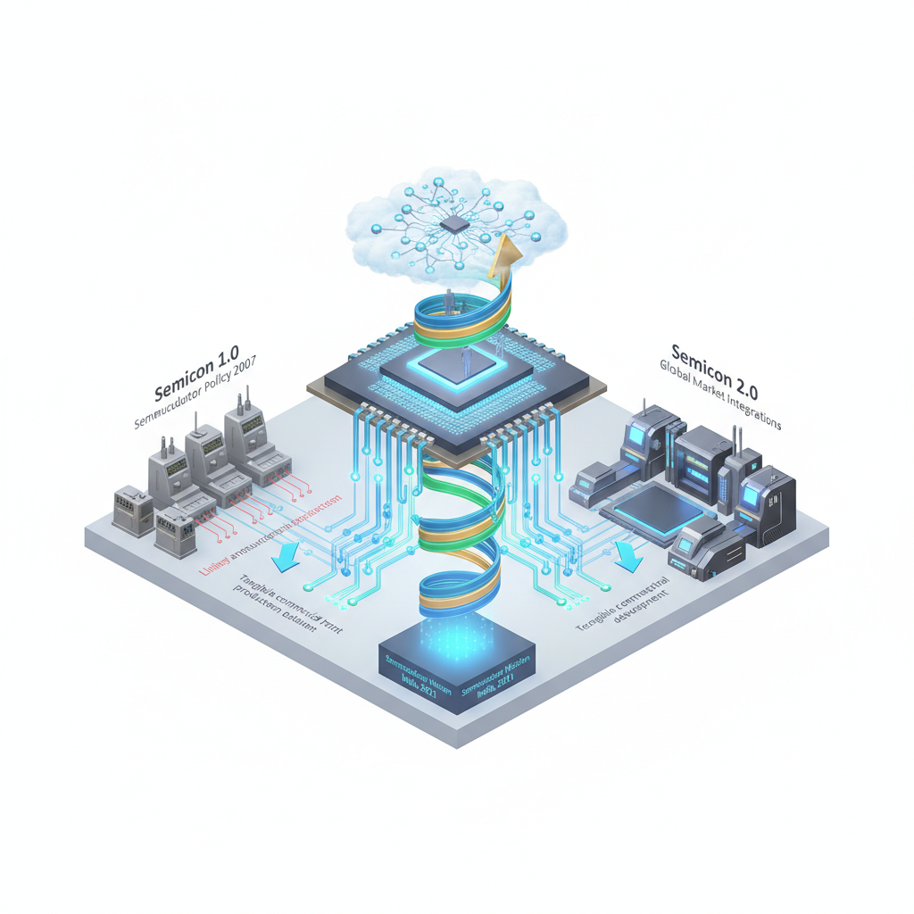
✎ Semiconductor Mission India aims to transform India from a semiconductor importer to a self-reliant global hub through Semicon 1.0 (foundation-building) and Semicon 2.0 (commercialisation and ecosystem deepening).
Subject Relevance — Where This Topic Fits
- GS Paper III — Indian Economy: Issues relating to Planning, Mobilisation of Resources, Growth, Development and Employment | GS Paper III — Industrial Policy and Promotion | GS Paper III — Science and Technology — Developments and their Applications and Effects in Everyday Life
- Prelims: Semiconductor Mission India, Semicon 2.0, SEMICON India 2026, Semiconductor Fabrication Unit (Fab), Semiconductor Packaging, Electronics Manufacturing Clusters (EMCs), Production-Linked Incentive (PLI) Scheme for Electronics, Semiconductor Laboratory (SCL) Mohali, Semiconductor Wafer Fabrication (FAB) Units
- Essay: Technological Self-Reliance: The Imperative of Building Domestic Semiconductor Capabilities, From ‘Make in India’ to ‘Make for the World’: The Role of High-Tech Manufacturing in India’s Growth Trajectory
Quick Revision: Semiconductor Mission India aims to transform India from a semiconductor importer to a self-reliant global hub through Semicon 1.0 (foundation-building) and Semicon 2.0 (commercialisation and ecosystem deepening).
Why is this in the news?
The conclusion of SEMICON India 2026 in New Delhi marked a significant milestone in India’s semiconductor journey, with industry stakeholders highlighting a shift from policy announcements to tangible commercial production and ecosystem development. The event underscored the transition from Semicon 1.0 to Semicon 2.0, characterised by increased investment commitments, strategic partnerships, and projected market growth, signalling a ‘positive spiral’ of localisation, skill development, and technological advancement in the sector.
Background
- India’s semiconductor policy framework has evolved through multiple phases, beginning with the Semiconductor Policy 2007, which offered fiscal incentives but yielded limited success due to global competition and high capital costs.
- The Semiconductor Mission India, launched in 2021, represents a strategic shift, aiming to establish India as a global hub for semiconductor design, manufacturing, and supply chain resilience.
- Semicon 1.0 focused on laying the groundwork through fiscal incentives, skill development, and infrastructure creation, while Semicon 2.0 emphasises deepening the ecosystem through commercialisation, localisation, and global partnerships.
- SEMICON India, an annual event organised by SEMI India and the India Electronics and Semiconductor Association (IESA), serves as a platform for industry collaboration, showcasing technological advancements and investment opportunities.
- Global semiconductor supply chain disruptions during the COVID-19 pandemic highlighted India’s vulnerability and the strategic necessity of building domestic semiconductor capabilities.
What is the Semiconductor Mission India and Semicon 2.0?
- The Semiconductor Mission India is a government-led initiative to position India as a global leader in semiconductor design, manufacturing, and supply chain, aligning with the ‘Atmanirbhar Bharat’ vision.
- The mission targets the entire semiconductor value chain: chip design (fabless), fabrication (fabs), assembly, testing, packaging (ATMP), materials, equipment, and end-user electronics manufacturing.
- Key objectives include reducing India’s import dependence for semiconductors, enhancing export competitiveness, and fostering innovation through R&D and skill development.
- The mission is implemented by a nodal agency, the India Semiconductor Mission (ISM), under the Ministry of Electronics and Information Technology (MeitY).
- Strategic partnerships with global semiconductor firms (e.g., Micron, AMD, Qualcomm) and domestic players (e.g., Tata Electronics, Vedanta) are critical to achieving scale and technological depth.
- Localisation efforts aim to develop domestic capabilities in semiconductor materials (e.g., silicon wafers), equipment (e.g., lithography machines), and advanced packaging technologies.
Key Features
| Feature | Significance |
|---|---|
| Semicon 2.0 Policy Framework | Transition from policy announcements to commercial production and ecosystem development in semiconductors, focusing on localisation and value addition. |
| SEMICON India 2026 | Fifth edition of the flagship event showcasing India’s semiconductor ecosystem, attracting global participation, investment commitments, and strategic partnerships. |
| Investment Commitments ($7 billion) | Demonstrates growing investor confidence in India’s semiconductor manufacturing, packaging, and design capabilities. |
| Ecosystem Spiral Model | Describes a self-reinforcing cycle where investment leads to manufacturing, supplier demand, localisation, skill development, and further investment. |
| EY-IESA Market Projection ($200 billion by 2035) | Highlights India’s potential as a major semiconductor market, driven by growth across the entire value chain. |
Why it Matters
Economic
- India’s semiconductor industry is transitioning from policy intent to commercial viability, reducing import dependency and enhancing self-reliance.
- Projected market size of $200 billion by 2035 positions semiconductors as a high-growth sector, contributing to GDP and employment generation.
- Foreign direct investment (FDI) inflows and global partnerships strengthen India’s position in the global semiconductor supply chain.
Strategic
- Semiconductor manufacturing is critical for national security, digital sovereignty, and technological autonomy in critical sectors like defence, telecommunications, and space.
- A robust semiconductor ecosystem reduces reliance on geopolitically sensitive supply chains, particularly in the context of global trade tensions.
- India’s participation in the global semiconductor value chain enhances its strategic leverage in international technology governance.
Industrial and Technological
- The shift from Semicon 1.0 (policy foundation) to Semicon 2.0 (ecosystem deepening) marks a maturing phase, with focus on fabs, advanced packaging, and materials.
- Collaboration between industry (SEMI India, IESA), government, and academia is fostering innovation and skill development in semiconductor design and manufacturing.
- The event’s scale (51,656 registrations, 52 countries) reflects India’s growing attractiveness as a semiconductor manufacturing hub.
Employment and Skill Development
- The positive spiral model implies sustained job creation across the semiconductor value chain, from fabrication to packaging and design.
- Skill development initiatives are integral to the ecosystem, addressing the demand for specialised talent in semiconductor technologies.
Challenges
1. High Capital Expenditure and Risk Aversion
- Semiconductor fabrication requires substantial upfront investment, with long gestation periods and high failure risks, deterring private sector participation without robust incentives.
- Global competition for semiconductor investments necessitates competitive fiscal and non-fiscal incentives to attract large-scale fabs.
UPSC Link: GS3: Industrial Policy and Investment Models
2. Supply Chain and Raw Material Dependencies
- India lacks critical semiconductor raw materials (e.g., silicon wafers, specialty gases) and relies heavily on imports, creating vulnerabilities in the supply chain.
- Establishing a domestic supply chain for materials and equipment is essential for reducing import dependence and ensuring resilience.
UPSC Link: GS3: Supply Chain Resilience and Atmanirbhar Bharat
3. Talent Shortage and Skill Gaps
- The semiconductor industry demands a highly skilled workforce, including engineers, technicians, and researchers, which India currently lacks in sufficient numbers.
- Academic-industry collaboration and vocational training programs are required to bridge the skill gap and meet industry demands.
UPSC Link: GS2: Education and Skill Development
4. Infrastructure and Ecosystem Readiness
- Developing semiconductor ecosystems requires robust infrastructure, including reliable power supply, water resources, and logistics networks.
- Land acquisition, regulatory clearances, and environmental compliance add to the complexity and timelines for setting up fabrication units.
UPSC Link: GS3: Infrastructure Development and Ease of Doing Business
5. Global Competition and Geopolitical Factors
- India competes with established semiconductor hubs like Taiwan, South Korea, and the US, which have mature ecosystems and government support.
- Geopolitical tensions and trade restrictions (e.g., export controls on advanced semiconductor technologies) pose risks to India’s integration into global value chains.
UPSC Link: GS2: International Relations and GS3: Globalisation and its Impact
Challenges — UPSC Perspective
| Issue | Concern |
|---|---|
| Capital Intensity | High upfront investment and long payback periods deter private sector participation. |
| Supply Chain Vulnerabilities | Dependence on imported raw materials and equipment creates supply chain risks. |
| Skill Deficit | Insufficient trained workforce in semiconductor design, fabrication, and packaging. |
| Infrastructure Gaps | Inadequate power, water, and logistics infrastructure for large-scale manufacturing. |
| Regulatory Hurdles | Complex land acquisition, environmental clearances, and compliance processes delay project execution. |
| Global Competition | Established semiconductor hubs offer mature ecosystems and government incentives, posing a challenge to India’s attractiveness. |
Government Initiatives — Must-Memorise for Prelims
- Semiconductor Mission India (SMI)
- Production-Linked Incentive (PLI) Scheme for Semiconductors and Display Manufacturing
Way Forward
- Accelerate the establishment of semiconductor fabrication units (fabs) through streamlined regulatory processes and fiscal incentives.
- Develop domestic capabilities in semiconductor materials, equipment, and advanced packaging to reduce import dependence.
- Strengthen academic-industry partnerships to address skill gaps through targeted training programs and research collaborations.
- Enhance infrastructure readiness, including reliable power supply, water resources, and logistics, in potential semiconductor hubs.
- Leverage global partnerships and technology transfers to fast-track ecosystem development and skill acquisition.
- Implement robust monitoring and evaluation mechanisms to track progress and address bottlenecks in the semiconductor mission.
- Promote R&D in semiconductor technologies to foster innovation and reduce reliance on imported technologies.
- Ensure policy stability and predictability to maintain investor confidence and attract long-term investments.
UPSC Value Addition
Keywords for Mains Answer-Writing
Semiconductor industry · Semicon 2.0 policy · SEMICON India 2026 · Semiconductor ecosystem · Electronics manufacturing · Localisation of supply chains · Investment in high-tech manufacturing · Intellectual property in semiconductors · Advanced packaging · Skill development in semiconductor technology · Industry-academia collaboration · Global semiconductor supply chain · Atmanirbhar Bharat in electronics · Public-private partnerships in R&D · IPR regime and semiconductor innovation
Concept Flow
Policy Announcements (Semicon 1.0) → Ecosystem Foundation → Investment Commitments and MoUs → Commercial Production Initiation → Manufacturing Expansion → Supplier Demand Creation → Supplier Demand → Localisation of Materials and Equipment → Localisation → Skill Development and Technology Adoption → Skill and Technology Development → Further Investment Attraction → Investment Attraction → Positive Spiral of Growth and Self-Reliance
Prelims Practice Questions
Q1. Consider the following statements regarding the semiconductor industry in India:
1. The SEMICON India 2026 event recorded over 50,000 registrations and participation from 52 countries.
2. The event witnessed investment commitments exceeding $10 billion.
3. The Semicon 2.0 policy aims to deepen the semiconductor ecosystem beyond foundational policy frameworks.
4. The EY-IESA report projected India’s semiconductor market to reach $200 billion by 2035.
How many of the above statements are correct?
- Only one
- Only two
- Only three
- All four
Answer: Only three — Statements 1, 3, and 4 are correct. Statement 2 is incorrect as the investment commitments were around $7 billion, not exceeding $10 billion.
Q2. Assertion (A): The Semicon 2.0 policy focuses on creating a self-sustaining semiconductor ecosystem through localisation and skill development.
Reason (R): The policy aims to reduce India’s dependence on imported semiconductor components by incentivising domestic manufacturing and R&D.
Options:
A. Both A and R are true, and R is the correct explanation of A.
B. Both A and R are true, but R is not the correct explanation of A.
C. A is true, but R is false.
D. A is false, but R is true.
- A
- B
- C
- D
Answer: A — Both the assertion and reason are true, and the reason correctly explains the assertion. The Semicon 2.0 policy indeed emphasises localisation, skill development, and reducing import dependence as core objectives.
Q3. Match the following terms associated with the semiconductor industry with their correct descriptions:
Column I
1. Semicon 2.0
2. SEMICON India
3. Advanced packaging
4. IPR regime
Column II
A. A biennial event showcasing the semiconductor ecosystem and facilitating B2B discussions.
B. A policy framework aimed at deepening the semiconductor ecosystem beyond foundational support.
C. Legal and institutional framework governing intellectual property rights in semiconductor design and innovation.
D. A technology segment involving high-end encapsulation and interconnection techniques for semiconductors.
Options:
1. 1-A, 2-B, 3-C, 4-D
2. 1-B, 2-A, 3-D, 4-C
3. 1-C, 2-D, 3-A, 4-B
4. 1-D, 2-C, 3-B, 4-A
- 1
- 2
- 3
- 4
Answer: 2 — 1-B (Semicon 2.0 is a policy framework), 2-A (SEMICON India is a biennial event), 3-D (Advanced packaging involves encapsulation and interconnection techniques), 4-C (IPR regime governs intellectual property rights).
Mains Practice Question
✍ ‘The development of India’s semiconductor ecosystem is not merely an industrial endeavour but a strategic imperative for technological sovereignty and economic resilience.’ Critically examine this statement with reference to the Semicon 2.0 policy and recent initiatives such as SEMICON India 2026. (15 Marks)
Approach: MODEL-ANSWER SKELETON:
1. **Introduction (2 marks)**: Define the semiconductor ecosystem and its strategic importance for India’s technological sovereignty and economic resilience. Mention the shift from Semicon 1.0 to Semicon 2.0.
2. **Semicon 2.0 Policy Framework (4 marks)**:
– Core objectives: deepening the ecosystem beyond foundational policy (e.g., incentives for fabs, design, packaging, materials, and equipment).
– Key provisions: Production Linked Incentive (PLI) schemes, Design Linked Incentive (DLI), and support for R&D.
– Institutional mechanisms: Role of MeitY, SEMI India, IESA, and state governments.
3. **SEMICON India 2026 and Ecosystem Building (4 marks)**:
– Highlight the scale of the event (registrations, exhibitors, MoUs, and investment commitments).
– Discuss the ‘positive spiral’ model: investment → manufacturing → supplier demand → localisation → skills → technology → further investment.
– Role of global participation and partnerships in accelerating ecosystem growth.
4. **Challenges and Critical Evaluation (3 marks)**:
– Structural challenges: high capital intensity, global competition, and supply chain vulnerabilities.
– Policy gaps: need for stronger IPR protection, talent development, and infrastructure.
– Balancing localisation with global integration: risks of protectionism vs. strategic autonomy.
5. **Conclusion (2 marks)**:
– Reiterate the strategic imperative of semiconductor self-reliance for India’s future.
– Emphasise the need for sustained public-private partnerships and global collaboration to realise the $200 billion market potential by 2035.
Source: orissapost.com
Generated by AanyaAi for educational purpose.
Related guides on our sites
- Current affairs for upsc 2026
- How to prepare for GS paper 1 for UPSC CSE mains exam
- Best UPSC coaching for IFOS exam
- Best mentorship programme for upsc

- India’s Semiconductor Ecosystem Enters Positive Spiral: SEMICON 2.0 Insights - September 24, 2026
- आईआईडब्ल्यूडब्ल्यू 2026: जल सुरक्षा के लिए नवाचार, जलवायु-लचीलेपन और डिजिटल समाधान - September 24, 2026
- IIWW 2026: AI & Climate-Resilient Water Solutions for UPSC Mains - September 24, 2026
No Comments