


31 Aug UPSC Alert: Rs 1.27 Lakh Crore Semicon 2.0 Scheme for Chip Ecosystem Boost
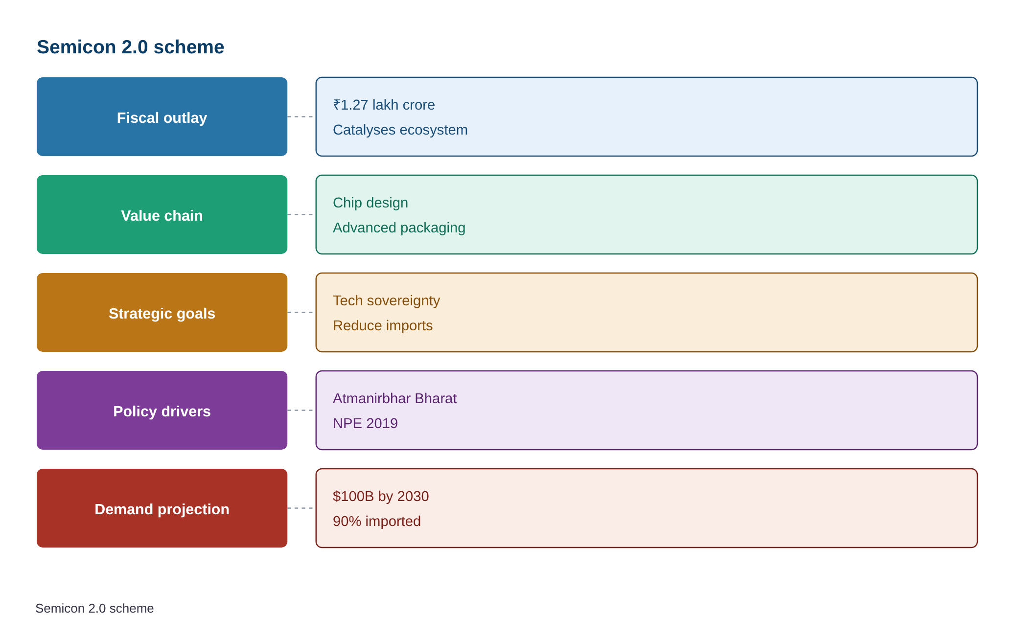
✎ The Semicon 2.0 Scheme, with a ₹1.27 lakh crore outlay, is India’s strategic intervention to build a self-reliant semiconductor ecosystem by incentivising design, fabrication, packaging, and materials across the entire value…
Subject Relevance — Where This Topic Fits
- GS Paper III — Economy: Industrial Policy, Manufacturing Sector, Investment Promotion | GS Paper III — Science & Technology: Emerging Technologies, R&D Ecosystem | GS Paper II — International Relations: Technology Diplomacy, Supply Chain Resilience
- Prelims: Semiconductor Mission India, Production Linked Incentive (PLI) Scheme for Electronics, Atmanirbhar Bharat Abhiyan, National Policy on Electronics 2019, Semiconductor Fabrication (Fab), Chip Design and Packaging, Intellectual Property (IP) Cores, System-on-Chip (SoC), Electronic Manufacturing Clusters (EMCs), Make in India 2.0
- Essay: Technological Sovereignty and National Security: The Imperative of Indigenous Semiconductor Capabilities, Balancing Globalisation and Self-Reliance: India’s Strategic Approach to Critical Technology
Quick Revision: The Semicon 2.0 Scheme, with a ₹1.27 lakh crore outlay, is India’s strategic intervention to build a self-reliant semiconductor ecosystem by incentivising design, fabrication, packaging, and materials across the entire value chain.
Why is this in the news?
The Union Government has notified the Semiconductor 2.0 Scheme with a financial outlay of ₹1.27 lakh crore to catalyse the development of a comprehensive semiconductor ecosystem in India. This initiative is a critical component of India’s broader strategy to achieve technological sovereignty, reduce import dependence, and position itself as a global hub for semiconductor design, manufacturing, and assembly. The scheme’s structured fiscal support across the entire value chain—from chip design to advanced packaging—aligns with India’s aspirations under the Atmanirbhar Bharat initiative and the National Policy on Electronics 2019.
Background
- India’s semiconductor demand is projected to exceed $100 billion by 2030, with over 90% currently met through imports, exposing vulnerabilities in critical infrastructure and defence systems.
- The global semiconductor supply chain is highly concentrated, with East Asia dominating fabrication and advanced packaging, necessitating diversification for strategic autonomy.
- The COVID-19 pandemic and geopolitical tensions (e.g., US-China trade war) highlighted the risks of supply chain disruptions, accelerating India’s push for indigenous semiconductor capabilities.
- The National Policy on Electronics 2019 and the Digital India initiative underscore the role of semiconductors in enabling digital transformation, IoT, and smart infrastructure across sectors.
What is the Semicon 2.0 Scheme?
- A scheme notified by the government with a total financial outlay of ₹1.27 lakh crore, designed to foster a resilient, sovereign, and globally competitive semiconductor ecosystem in India.
- The scheme adopts a value-chain approach, providing fiscal support across six segments: designing of chips by Indian firms, setting up units for capital equipment required for chip production, semiconductor fabs, outsourced semiconductor assembly and test (OSAT) units, compound semiconductors, and silicon photonics.
- The scheme prioritises indigenous development of semiconductor Intellectual Property (IP) cores, Chips, System-on-Chips (SoCs), and modules, with a focus on technologies critical for national security, defence, and strategic infrastructure.
Key Features
| Feature | Significance |
|---|---|
| Outlay of ₹1.27 lakh crore | Provides substantial fiscal support to cover the entire semiconductor value chain, including design, fabrication, and packaging. |
| Six-segment coverage | Ensures comprehensive development across chip design, capital equipment, semiconductor fabs, assembly, packaging, and testing. |
| Focus on sovereign technologies | Aims to build resilient and trusted semiconductor technologies for national strategic and critical infrastructure. |
| Development of IP cores and SoCs | Targets local development of semiconductor Intellectual Property (IP) cores, Chips, System-on-Chips (SoCs), and modules for electronic products. |
| Building block development | Includes standard IPs for Compute, Memory, RF, Power, Networking, Sensors, etc., to support diverse applications. |
Why it Matters
Economic
- Stimulates investment in high-tech manufacturing, potentially increasing India’s share in the global semiconductor market.
- Encourages domestic and foreign investment in semiconductor fabrication and ancillary industries, creating employment opportunities.
- Reduces import dependency for critical electronic components, improving the trade balance over time.
Strategic
- Enhances India’s technological sovereignty by reducing reliance on imported semiconductor chips for critical infrastructure.
- Supports the development of indigenous semiconductor design and manufacturing capabilities for defense, space, and other strategic sectors.
- Aligns with national priorities for self-reliance in electronics manufacturing under initiatives like ‘Make in India’.
Industrial
- Facilitates the establishment of semiconductor fabrication units (fabs) in India, fostering a robust ecosystem.
- Promotes the growth of ancillary industries such as capital equipment manufacturing and chip packaging/testing.
- Encourages collaboration between academia, industry, and research institutions for innovation in semiconductor technology.
Challenges
1. High Capital Requirements
- Semiconductor fabrication requires massive upfront capital investment, posing financial risks for private players.
- Long gestation periods for returns may deter investors despite government incentives.
UPSC Link: GS3: Industrial Policy & Investment Models
2. Technological Gap
- India lacks mature semiconductor manufacturing infrastructure compared to global leaders like the US, South Korea, and Taiwan.
- Dependence on imported technology and equipment for advanced nodes (e.g., sub-10nm) remains a challenge.
UPSC Link: GS3: Science & Technology
3. Skilled Workforce Shortage
- Limited availability of specialized talent in semiconductor design, fabrication, and testing.
- Need for targeted education and skill development programs to bridge the talent gap.
UPSC Link: GS2: Education & Skill Development
4. Global Competition
- Competition from established semiconductor hubs with mature ecosystems and lower production costs.
- Risk of overcapacity if global demand does not align with domestic production targets.
UPSC Link: GS2: International Trade & Investment
5. Policy and Regulatory Hurdles
- Complexity in obtaining clearances for setting up semiconductor fabs due to land, environmental, and regulatory requirements.
- Need for streamlined approval processes to expedite project implementation.
UPSC Link: GS2: Governance & Administration
Challenges — UPSC Perspective
| Issue | Concern |
|---|---|
| Capital Intensity | High upfront investment and long payback periods deter private participation. |
| Technology Dependence | Reliance on imported technology and equipment for advanced semiconductor nodes. |
| Talent Shortage | Limited availability of specialized workforce in semiconductor design and fabrication. |
| Global Competition | Established semiconductor hubs pose stiff competition to new entrants. |
| Regulatory Delays | Complex approval processes may slow down project execution. |
| Infrastructure Gaps | Inadequate supporting infrastructure for water, power, and logistics in potential fab locations. |
Government Initiatives — Must-Memorise for Prelims
- Semiconductor Mission (India Semiconductor Mission – ISM)
- Production Linked Incentive (PLI) Scheme for Large Scale Electronics Manufacturing
- Modified Electronics Manufacturing Clusters (EMC 2.0) Scheme
Way Forward
- Establish dedicated semiconductor manufacturing zones with plug-and-play infrastructure to reduce setup costs.
- Expand skill development programs in collaboration with IITs, NITs, and industry partners to address the talent shortage.
- Accelerate R&D in semiconductor technology through public-private partnerships and academia-industry linkages.
- Streamline regulatory approvals for semiconductor fabs by creating a single-window clearance mechanism.
- Enhance global partnerships to facilitate technology transfer and access to advanced manufacturing equipment.
- Monitor and evaluate the scheme’s progress through periodic audits to ensure efficient utilization of funds.
- Promote domestic demand for locally manufactured semiconductors through government procurement policies.
- Develop a robust supply chain ecosystem for raw materials and components to reduce import dependency.
UPSC Value Addition
Keywords for Mains Answer-Writing
Semiconductor Mission India · Semicon 2.0 Scheme · Semiconductor manufacturing ecosystem · Production Linked Incentive (PLI) Scheme · Semiconductor fabs · Chip design and packaging · National Semiconductor Strategy · Critical infrastructure and strategic autonomy · Atmanirbhar Bharat in electronics · Electronic System Design and Manufacturing (ESDM)
Concept Flow
Global semiconductor demand surge → Government recognises strategic importance → Formulation of Semicon 2.0 scheme → Fiscal outlay of ₹1.27 lakh crore → Coverage of entire value chain (design to packaging) → Focus on sovereign technologies → Development of IP cores and SoCs → Establishment of semiconductor fabs → Employment generation and technological self-reliance.
Prelims Practice Questions
Q1. Consider the following statements regarding the Semicon 2.0 Scheme notified by the Government of India:
1. The scheme has a total financial outlay of Rs 1.27 lakh crore.
2. It exclusively focuses on semiconductor fabrication units (fabs) and excludes chip design and packaging.
3. The scheme aims to develop sovereign semiconductor technologies for national strategic and critical infrastructure.
How many of the above statements are correct?
- Only one
- Only two
- All three
- None
Answer: All three — Statements 1 and 3 are correct. Statement 2 is incorrect as the scheme covers the entire value chain, including chip design, fabrication, packaging, and testing.
Q2. Assertion (A): The Semicon 2.0 Scheme is a part of India’s broader strategy to achieve self-reliance in semiconductor manufacturing.
Reason (R): The scheme provides fiscal support across the semiconductor value chain, including design, fabrication, and packaging, to reduce import dependence.
In the context of the above two statements, which one of the following is correct?
- Both A and R are true, and R is the correct explanation of A.
- Both A and R are true, but R is not the correct explanation of A.
- A is true, but R is false.
- A is false, but R is true.
Answer: Both A and R are true, and R is the correct explanation of A. — Both the assertion and reason are true. The Semicon 2.0 Scheme is indeed part of India’s self-reliance strategy (A), and the reason correctly explains the scheme’s role in providing fiscal support across the value chain (R).
Q3. Match the following segments of the Semicon 2.0 Scheme (Column I) with their respective objectives (Column II):
Column I:
A. Semiconductor fabs
B. Chip design
C. Assembly, packaging, and testing
D. Capital equipment for chip production
Column II:
1. Development of indigenous Intellectual Property (IP) cores and System-on-Chips (SoCs)
2. Establishment of high-technology fabrication units
3. Enhancement of end-of-line manufacturing processes
4. Provision of machinery and tools for semiconductor manufacturing
Select the correct match:
- A-2, B-1, C-3, D-4
- A-1, B-2, C-3, D-4
- A-3, B-1, C-2, D-4
- A-4, B-2, C-1, D-3
Answer: A-2, B-1, C-3, D-4 — The correct matches are: A-2 (Semiconductor fabs aim to establish high-technology fabrication units), B-1 (Chip design focuses on developing indigenous IP cores and SoCs), C-3 (Assembly, packaging, and testing enhance end-of-line manufacturing processes), and D-4 (Capital equipment provides machinery and tools for semiconductor manufacturing).
Mains Practice Question
✍ The Semicon 2.0 Scheme, with a financial outlay of Rs 1.27 lakh crore, represents a pivotal intervention in India’s quest for strategic autonomy in semiconductor technologies. Critically analyse the scheme’s objectives, institutional mechanisms, and potential challenges in achieving its goals. Also, examine how the scheme aligns with India’s broader Atmanirbhar Bharat and Electronic System Design and Manufacturing (ESDM) policies. (15 Marks)
Approach: MODEL-ANSWER SKELETON:
1. **Introduction (2 marks)**: Define the Semicon 2.0 Scheme, its outlay (Rs 1.27 lakh crore), and its placement within India’s broader semiconductor and ESDM policies. Mention the scheme’s division into six segments (chip design, capital equipment, fabs, assembly, packaging, and testing).
2. **Objectives and Institutional Framework (4 marks)**:
– **Strategic Autonomy**: Focus on sovereign semiconductor technologies, indigenous IP cores, SoCs, and modules for national strategic and critical infrastructure.
– **Fiscal Support**: Outline the fiscal incentives provided across the value chain (design, fabrication, packaging, and testing).
– **Institutional Mechanisms**: Reference the role of the Ministry of Electronics and Information Technology (MeitY), the Semiconductor Mission India, and the Production Linked Incentive (PLI) Scheme in implementation.
3. **Alignment with Atmanirbhar Bharat and ESDM (3 marks)**:
– **Atmanirbhar Bharat**: Link the scheme to the broader goal of reducing import dependence in critical technologies and enhancing domestic manufacturing capabilities.
– **ESDM Policy**: Discuss how the scheme complements the ESDM policy, which aims to position India as a global hub for electronics manufacturing.
4. **Potential Challenges (4 marks)**:
– **Technological and Financial Risks**: High capital intensity, long gestation periods, and technological obsolescence in semiconductor manufacturing.
– **Global Competition**: Competition from established semiconductor hubs (e.g., Taiwan, South Korea, USA, and China) and the need to attract global players.
– **Skill Gaps**: Shortage of skilled manpower in semiconductor design, fabrication, and advanced packaging.
– **Supply Chain Dependencies**: Reliance on imported raw materials, equipment, and intermediate goods.
5. **Conclusion (2 marks)**: Summarise the scheme’s significance in achieving strategic autonomy while acknowledging the challenges. Provide a balanced view on its potential success, citing examples of past initiatives (e.g., PLI Scheme for electronics) and their outcomes.
Source: orissapost.com
Generated by AanyaAi for educational purpose.
Related guides on our sites
- Best PSIR optional coaching for upsc
- Best PSIR optional teacher for upsc
- Best teacher of PSIR optional for upsc
- Best PSIR optional coaching in delhi for UPSC


No Comments