


31 Aug Govt Launches Rs 1.27 Lakh Cr Semicon 2.0 Scheme to Boost Chip Ecosystem
✎ The Semiconductor 2.0 Scheme is a ₹1.27 lakh crore fiscal framework to build a self-reliant, resilient, and sovereign semiconductor ecosystem in India, covering design, fabrication, packaging, and capital equipment manufacturing…
Subject Relevance — Where This Topic Fits
- GS Paper II — International Relations (Global Supply Chain Resilience) | GS Paper III — Economy (Industrial Policy, Manufacturing Sector, Investment)
- Prelims: Semiconductor Mission India, Production-Linked Incentive (PLI) Scheme, Atmanirbhar Bharat Abhiyaan, Electronic Manufacturing Clusters (EMC), Semiconductor Fabrication Units (Fabs), Intellectual Property (IP) Cores, System-on-Chip (SoC), Chip Design and Packaging
- Essay: India’s Technological Sovereignty: The Imperative of a Robust Semiconductor Ecosystem, Balancing Globalisation and Self-Reliance in High-Tech Manufacturing
Quick Revision: The Semiconductor 2.0 Scheme is a ₹1.27 lakh crore fiscal framework to build a self-reliant, resilient, and sovereign semiconductor ecosystem in India, covering design, fabrication, packaging, and capital equipment manufacturing, with a focus on indigenous IP development and strategic sectors.
Why is this in the news?
The Government of India has notified the Semiconductor 2.0 Scheme with a financial outlay of ₹1.27 lakh crore to catalyse the development of a comprehensive semiconductor ecosystem in India. This initiative is a critical component of India’s broader strategy to reduce import dependence in critical technologies, enhance domestic value addition, and position the country as a global hub for semiconductor design, manufacturing, and innovation. The scheme’s structured fiscal support across the semiconductor value chain underscores its strategic importance in the context of geopolitical supply chain realignments and India’s aspirations for technological self-reliance.
Background
- The semiconductor industry is a foundational pillar of the modern digital economy, underpinning sectors such as electronics, telecommunications, automotive, defence, and healthcare.
- India’s semiconductor demand is projected to reach $100 billion by 2030, with over 90% of chips currently imported, exposing the economy to supply chain vulnerabilities and geopolitical risks.
- The Semiconductor Mission India was launched in 2021 with an initial outlay of ₹76,000 crore to attract investments in semiconductor fabrication, design, and packaging units.
- Global semiconductor supply chains are increasingly characterised by geopolitical fragmentation, with major economies (e.g., the US, EU, and China) offering substantial incentives to localise chip production.
- The Make in India initiative has identified electronics manufacturing, including semiconductors, as a key growth sector to achieve a $5 trillion economy.
- The scheme aligns with the Production-Linked Incentive (PLI) Scheme and the Design-Linked Incentive (DLI) Scheme to create a holistic ecosystem for chip manufacturing and innovation.
What is the Semiconductor 2.0 Scheme?
- The Semiconductor 2.0 Scheme is a centrally sponsored fiscal incentive programme with a total outlay of ₹1.27 lakh crore, notified to accelerate the development of India’s semiconductor ecosystem across the entire value chain.
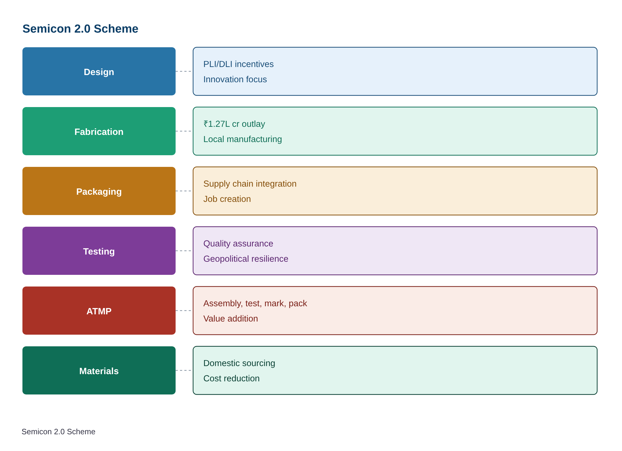
- The scheme is structured into six verticals: (1) Semiconductor Design, (2) Semiconductor Fabrication (Fabs), (3) Semiconductor Packaging and Testing, (4) Semiconductor Capital Equipment Manufacturing, (5) Semiconductor Assembly, and (6) Electronic System Design and Manufacturing (ESDM) support.
- Fiscal support under the scheme includes direct subsidies, viability gap funding, and interest subvention to eligible entities, with a focus on indigenous development of semiconductor Intellectual Property (IP) cores, System-on-Chips (SoCs), and modules.
- The scheme prioritises the development of ‘trusted’ and ‘sovereign’ semiconductor technologies, particularly for critical infrastructure, defence, and strategic applications.
- Target segments include Compute, Memory, RF (Radio Frequency), Power, Networking, and Sensor technologies, with standard IPs to be developed for these domains.
- The scheme encourages collaboration between domestic firms, academic institutions, and research organisations to foster innovation and skill development in semiconductor design and manufacturing.
- Eligibility criteria and application processes are governed by the Ministry of Electronics and Information Technology (MeitY), with transparent evaluation mechanisms to ensure accountability and efficiency.
- The scheme is designed to complement existing initiatives such as the PLI Scheme for Large Scale Electronics Manufacturing and the Scheme for Promotion of Manufacturing of Electronic Components and Semiconductors (SPECS).
Key Features
| Feature | Significance |
|---|---|
| Outlay of ₹1.27 lakh crore | Provides substantial fiscal support to develop a self-reliant semiconductor ecosystem, aligning with national strategic priorities. |
| Six-segment coverage | Encompasses chip design, capital equipment manufacturing, semiconductor fabrication, assembly, packaging, and testing, ensuring end-to-end ecosystem development. |
| Fiscal incentives for design and manufacturing | Supports Indian firms in developing semiconductor IP cores, SoCs, and modules, fostering indigenous technological sovereignty. |
| Focus on strategic and critical infrastructure | Targets technologies essential for national security, digital infrastructure, and critical sectors like defence, telecom, and healthcare. |
| Development of standard IPs | Encourages creation of reusable IP blocks for compute, memory, RF, power, networking, and sensors, reducing dependency on foreign designs. |
Why it Matters
Economic
- Reduces import dependence on semiconductor chips, projected to save foreign exchange outflows of approximately $10 billion annually by 2030.
- Estimates suggest the scheme could generate 200,000 direct and indirect jobs in the semiconductor value chain over the next decade.
- Enhances India’s position in global electronics manufacturing, complementing existing PLI schemes for electronics and IT hardware.
Strategic
- Strengthens national security by reducing vulnerabilities in critical infrastructure reliant on imported semiconductor components.
- Supports the ‘Atmanirbhar Bharat’ initiative by promoting indigenous design and manufacturing capabilities in high-tech sectors.
- Aligns with global trends in semiconductor reshoring, positioning India as a trusted manufacturing hub for allied nations.
Technological
- Fosters innovation in semiconductor design, particularly in niche areas like low-power chips, AI accelerators, and IoT devices.
- Encourages collaboration between academia (e.g., IITs, IISc) and industry for R&D in advanced semiconductor technologies.
- Promotes the development of domestic semiconductor testing and packaging infrastructure, a critical bottleneck in the value chain.
Geopolitical
- Reduces reliance on semiconductor supply chains dominated by a few countries, mitigating geopolitical risks in technology access.
- Enhances India’s bargaining power in global semiconductor trade negotiations and partnerships with multinational corporations.
Challenges
1. High Capital and Technology Barriers
- Semiconductor fabrication requires investments exceeding ₹50,000 crore per fab, with long gestation periods (5–7 years) before profitability.
- Access to cutting-edge fabrication technology (e.g., 3nm nodes) remains restricted due to export controls by advanced economies like the US and Japan.
- Limited domestic availability of skilled manpower in semiconductor design, fabrication, and advanced packaging.
UPSC Link: GS3: Industrial Policy
2. Supply Chain and Infrastructure Gaps
- India lacks a robust ecosystem for raw material supply (e.g., silicon wafers, specialty gases, and chemicals) critical for semiconductor manufacturing.
- Inadequate infrastructure for water, electricity, and waste management in potential semiconductor hubs (e.g., Gujarat, Tamil Nadu, Karnataka).
- Dependence on imports for capital equipment (e.g., lithography machines) due to limited domestic manufacturing capabilities.
UPSC Link: GS3: Infrastructure
3. Global Competition and Subsidies
- Competition from countries like the US (CHIPS Act), China (subsidies up to $150 billion), and South Korea (K-Semicon) with aggressive incentive structures.
- Risk of overcapacity in the global semiconductor market, leading to price wars and reduced profitability for new entrants.
- Need to align with global standards (e.g., ISO 26262 for automotive chips) to ensure market access in regulated sectors.
UPSC Link: GS2: International Relations
4. Policy and Regulatory Hurdles
- Complexity in land acquisition, environmental clearances, and labour regulations for large-scale semiconductor projects.
- Uncertainty in long-term fiscal support due to budgetary constraints and competing priorities in public expenditure.
- Coordination challenges between central ministries (e.g., MeitY, DPIIT, DST) and state governments for seamless implementation.
UPSC Link: GS2: Governance
5. Market and Demand Risks
- Fluctuations in global demand for electronics, particularly in consumer devices, can impact the viability of semiconductor projects.
- Dependence on a few large customers (e.g., Apple, Samsung) for off-take agreements, creating revenue concentration risks.
- Need for sustained R&D investment to keep pace with rapid technological obsolescence in the semiconductor industry.
UPSC Link: GS3: Technology Missions
Challenges — UPSC Perspective
| Issue | Concern |
|---|---|
| High Capital Requirements | Limited private sector appetite for high-risk, long-gestation investments without assured returns. |
| Technology Access Restrictions | Export controls on advanced semiconductor equipment impede domestic fabrication capabilities. |
| Skill Shortages | Insufficient domestic talent pool in semiconductor design, fabrication, and advanced packaging. |
| Infrastructure Bottlenecks | Inadequate water, power, and waste management infrastructure near potential semiconductor hubs. |
| Global Competition | Aggressive subsidies from other nations may render Indian projects uncompetitive in cost terms. |
| Policy Coordination Gaps | Fragmented implementation across central and state governments may delay project execution. |
Government Initiatives — Must-Memorise for Prelims
- Semicon India Programme (2021)
- Production-Linked Incentive (PLI) Scheme for Large Scale Electronics Manufacturing
- Modified Electronics Manufacturing Clusters (EMC 2.0) Scheme
Way Forward
- Establish dedicated semiconductor manufacturing zones with pre-approved land, single-window clearances, and dedicated infrastructure corridors.
- Expand collaboration with international semiconductor firms (e.g., Intel, TSMC) for technology transfer and joint ventures in fabrication.
- Strengthen academia-industry linkages through centres of excellence (e.g., IISc, IITs) for semiconductor R&D and talent development.
- Develop a phased roadmap for indigenous manufacturing of critical inputs (e.g., silicon wafers, specialty gases) to reduce import dependence.
- Create a sovereign semiconductor fund to provide patient capital for high-risk, long-gestation projects in fabrication and advanced packaging.
- Align with global standards (e.g., ISO, IEC) and certifications to ensure market access for domestically manufactured chips.
- Enhance skill development initiatives through partnerships with vocational training institutes and international certification bodies.
- Monitor and evaluate the scheme’s progress via quarterly reports on disbursements, employment generation, and technological milestones.
UPSC Value Addition
Keywords for Mains Answer-Writing
Semiconductor Mission 2.0 · Semiconductor Manufacturing Ecosystem · Semiconductor Design and Fabrication · Semiconductor Intellectual Property (IP) Cores · System-on-Chip (SoC) · National Semiconductor Strategy · Atmanirbhar Bharat in Electronics · Semiconductor Packaging and Testing · Capital Equipment for Semiconductors · Semiconductor Value Chain · Trusted and Sovereign Semiconductor Technologies · Semiconductor Policy Support · Semiconductor Manufacturing Incentives · Semiconductor Supply Chain Resilience
Concept Flow
Global semiconductor supply chain disruptions → Government recognises strategic vulnerability → Formulation of Semicon 2.0 scheme → Allocation of ₹1.27 lakh crore → Incentives across six segments (design, fab, packaging, etc.) → Establishment of domestic semiconductor ecosystem → Reduction in import dependence → Strengthening of ‘Atmanirbhar Bharat’ → Enhanced national security and economic resilience.
Prelims Practice Questions
Q1. Consider the following statements regarding the Semicon 2.0 scheme recently notified by the Government of India:
1. The scheme has an outlay of Rs 1.27 lakh crore.
2. It covers only the fabrication of semiconductor chips.
3. The scheme provides fiscal support for chip design, fabrication, packaging, and testing.
4. It aims to develop trusted and sovereign semiconductor technologies.
How many of the above statements are correct?
- Only one
- Only two
- Only three
- All four
Answer: All four — Statements 1, 3, and 4 are correct. Statement 2 is incorrect as the scheme covers the entire value chain including design, fabrication, packaging, and testing.
Q2. Assertion (A): The Semicon 2.0 scheme aims to build resilient and sovereign semiconductor technologies.
Reason (R): The scheme provides fiscal support across the entire semiconductor value chain, including design, fabrication, and packaging.
Options:
A. Both A and R are true, and R is the correct explanation of A.
B. Both A and R are true, but R is not the correct explanation of A.
C. A is true, but R is false.
D. A is false, but R is true.
Answer: ? — Both the Assertion (A) and Reason (R) are true. The Reason (R) correctly explains the Assertion (A) as the fiscal support across the value chain is intended to achieve the goal of resilient and sovereign technologies.
Q3. Which of the following is NOT a segment covered under the Semicon 2.0 scheme for the semiconductor ecosystem?
A. Chip design by Indian firms
B. Setting up units for capital equipment required for chip production
C. Direct financial support to consumers for purchasing electronic devices
D. Semiconductor fabs, chip assembly, packaging, and testing
- A
- B
- C
- D
Answer: C — The Semicon 2.0 scheme covers chip design, capital equipment, semiconductor fabs, assembly, packaging, and testing. It does not provide direct financial support to consumers for purchasing electronic devices.
Mains Practice Question
✍ The Government of India has notified the Semicon 2.0 scheme with an outlay of Rs 1.27 lakh crore to bolster the semiconductor ecosystem in India. Critically examine the significance of this scheme in the context of India’s strategic autonomy, economic growth, and global semiconductor supply chain dynamics. Also, outline the key segments of the scheme and their potential impact on the semiconductor value chain. (15 Marks)
Approach: MODEL-ANSWER SKELETON:
1. **Introduction**: Define the semiconductor ecosystem and its critical role in modern electronics, digital infrastructure, and strategic sectors (defence, space, telecom, automotive). Highlight India’s current dependence on imported semiconductors and the vulnerabilities in the global supply chain.
2. **Strategic Autonomy**: Discuss how the scheme aligns with India’s goal of achieving self-reliance (Atmanirbhar Bharat) in critical technologies. Explain the concept of ‘trusted and sovereign semiconductor technologies’ and how the scheme aims to reduce import dependence.
3. **Economic Growth**: Analyse the potential economic benefits, including job creation, export opportunities, and attracting foreign direct investment (FDI) in high-tech manufacturing. Reference the multiplier effect on ancillary industries (e.g., capital equipment, materials).
4. **Global Semiconductor Supply Chain**: Examine India’s position in the global semiconductor value chain. Discuss how the scheme positions India as a competitive hub for semiconductor design, fabrication, and packaging, leveraging India’s strengths in IT services and engineering talent.
5. **Key Segments of the Scheme**:
– **Chip Design**: Support for Indian firms to develop semiconductor Intellectual Property (IP) cores and System-on-Chips (SoCs).
– **Semiconductor Fabs**: Incentives for establishing fabrication units to reduce reliance on imports.
– **Capital Equipment**: Development of domestic capabilities for manufacturing equipment required in semiconductor production.
– **Packaging and Testing**: Strengthening India’s role in the back-end of the semiconductor value chain.
6. **Challenges and Criticisms**: Address potential challenges such as high capital intensity, competition from established semiconductor hubs (e.g., Taiwan, South Korea), and the need for a skilled workforce. Discuss the role of public-private partnerships and the importance of sustained policy support.
7. **Conclusion**: Summarise the scheme’s potential to transform India’s semiconductor ecosystem and its broader implications for India’s technological sovereignty and economic resilience. Emphasise the need for effective implementation and continuous innovation.
Source: orissapost.com
Generated by AanyaAi for educational purpose.
Related guides on our sites
- Best PSIR optional coaching for upsc
- Best PSIR optional teacher for upsc
- Best teacher of PSIR optional for upsc
- Best PSIR optional coaching in delhi for UPSC

- माई भारत अभियान: ग्राम सेवा एवं खेल दिवस के तहत गांवों में Nasha Mukt Yuva Abhiyan - October 24, 2026
- Odisha’s Zero Casualty Plan as Cyclone Threatens: UPSC Geography Insights - October 24, 2026
- आरबीआई का ओडिशा डेटा सेंटर: अर्थव्यवस्था के लिए क्यों है महत्वपूर्ण? - October 24, 2026

No Comments